Lumped-element transmission line in multi-layered substrate

a transmission line and multi-layered technology, applied in the direction of high frequency circuit adaptation, one-port network, inductance, etc., can solve the problems of large circuit area, large physical length of the required transmission line, and insufficient so as to improve the frequency response of the lumped-element transmission line, wide frequency bandwidth, and reduce the circuit area of the transmission line

Inactive Publication Date: 2006-02-21
CHI MEI COMM SYST INC
View PDF10 Cites 9 Cited by
  • Summary
  • Abstract
  • Description
  • Claims
  • Application Information

AI Technical Summary

Benefits of technology

[0009]It is an advantage of the claimed invention that utilization of the mutual inductance improves frequency response of the lumped-element transmission line for a wide-band application. In the claimed invention, the circuit area of the transmission line is reduced by adopting the T-equivalent circuit model, and the associated frequency response close to that of an ideal transmission line for a wider frequency bandwidth is obtained. As transmission lines are widely used as building blocks in RF circuit design, a significant savings in circuit area, and hence cost in manufacturing, is obtained.

Problems solved by technology

However, the required physical lengths of these transmission lines are often quite long, such that they will occupy large circuit areas especially for low frequency applications.
Utilizing the meander line structure reduces the size of the required transmission line, but the resulting circuit area is still too large for the requirements of modern wireless handheld devices.
These limit the usage of these equivalent-circuit models to narrow band applications.
There have been many approaches to try to solve the aforementioned problem but the improvement is limited.
In addition, the poor frequency response of conventional lumped-element transmission line implementations becomes one of the thresholds in developing wide frequency band RF circuits.

Method used


Image

  • Lumped-element transmission line in multi-layered substrate
  • Lumped-element transmission line in multi-layered substrate
  • Lumped-element transmission line in multi-layered substrate

Examples


first embodiment

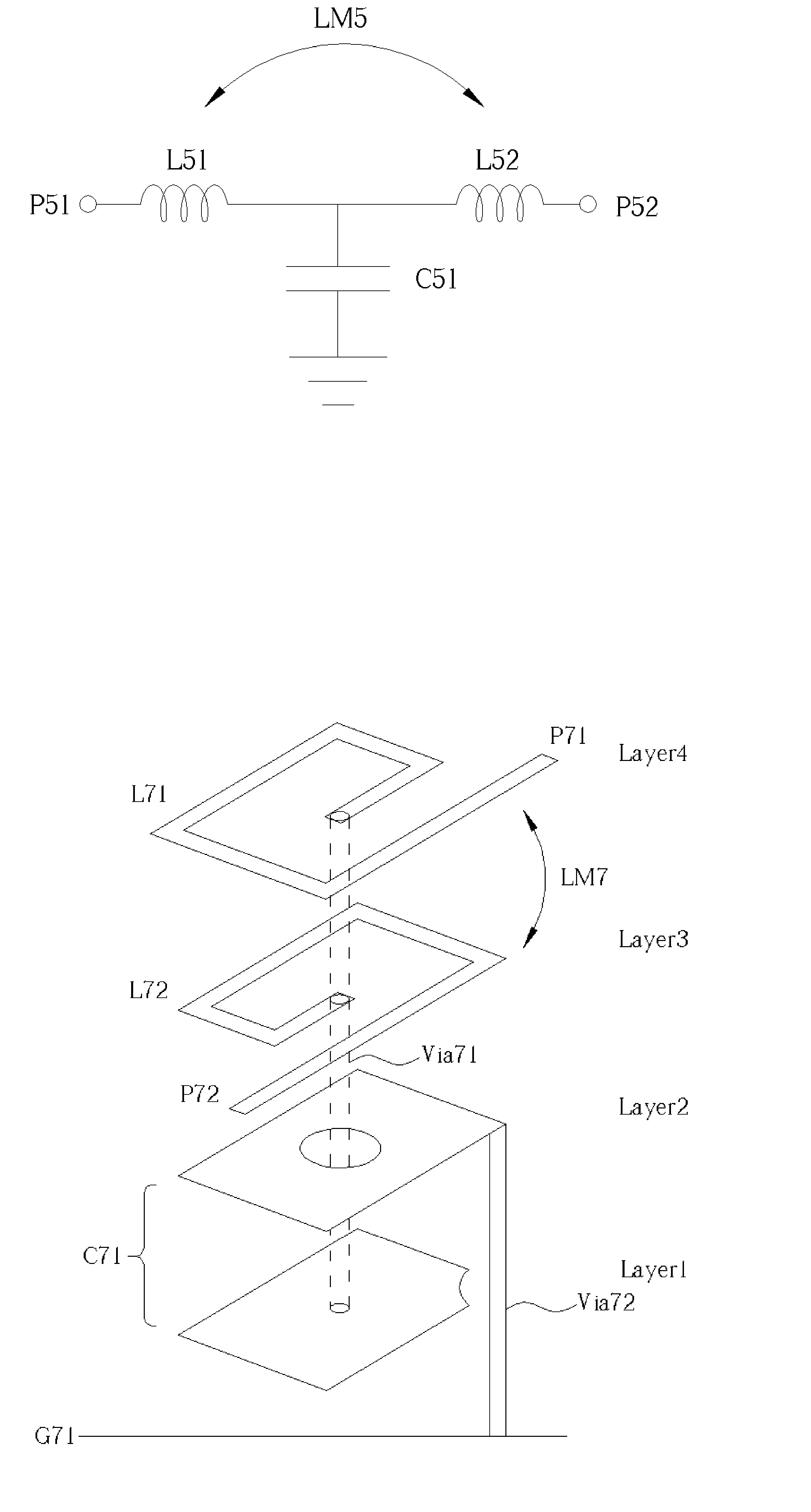
[0024]The primary reason for adopting lumped-element transmission lines is to reduce circuit area. The utilization of mutual inductance in the present invention helps to widen the applicable frequency range of the lumped-element transmission line. It is known that the mutual inductance relates to the relative distance and geometrical relations between two inductors. Therefore, it is very applicable to implement the present invention in a 3-dimensional structure such as a multi-layered substrate. Please refer to FIG. 7. FIG. 7 shows the present invention transmission line realized in a multi-layered substrate (layers 1–4) with a bottom ground plane G71. FIG. 7 illustrates inductors L71 and L72, a capacitor C71, and vias Via71 and Via72 penetrating the substrate and connecting different layers. The inductors L71 and L72 are realized with rectangular conductive spirals on layer 4 and layer 3 respectively. The inductor L72 is electrically connected to the inductor L71 in series through ...

second embodiment

[0025]FIG. 9 shows the present invention transmission line realized in a multi-layered substrate with both a top ground plane G92 and a bottom ground plane G91. FIG. 9 illustrates inductors L91 and L92, a capacitor C91, and vias Via91, Via92, and Via93 penetrating the substrate and connecting different layers. The inductors L91 and L92 are realized by conductive circular spirals on layer 4 and layer 3 respectively. The inductor L92 is electrically connected to the inductor L91 in series through the via Via91 penetrating the substrate. The capacitor C91 comprises two sub capacitors C911 and C912 shunt-connected to each other, such that each of them can be made smaller. The capacitor C911 comprises two plates formed on layer 1 and layer 2 of the multi-layered substrate, in which the plate formed on layer 2 is connected to the ground plane G91 through the via Via92 and the plate formed on layer 1 is connected to the via Via91. The capacitor C912 comprises two plates formed on a layer 5...

third embodiment

[0026]Shown in FIG. 11 and FIG. 12 are alternative realizations of the equivalent-circuit model in FIG. 5. Please refer to FIG. 11. FIG. 11 shows the present invention transmission line realized in a multi-layered substrate with a bottom ground plane G111. FIG. 11 illustrates inductors L111 and L112, a capacitor C111, and vias Via111 and Via112 penetrating the substrate and connecting different layers. The inductors L111 and L112 are realized by octagonal spirals on layer 2, and the inductor L112 is electrically connected to the inductor L111 in series at an end. The inductor L111 connects to a port P111 formed in layer 3 through the via Via111. The capacitor C111 is formed between a plate on layer 1 and the ground plane G111. The plate formed on layer 1 is connected to the via Via 112, which also connects to the end of the inductor L112 at which the inductor L112 is electrically connected to the inductor L111. Note that the orientations of inductors L111 and L112 are the same, thou...


PUM

PropertyMeasurementUnit
mutual inductanceaaaaaaaaaa
shapeaaaaaaaaaa
frequencyaaaaaaaaaa

Abstract

A lumped-element transmission line is formed in a multi-layered substrate. A mutual inductance between first and second inductors in a T-equivalent circuit model is enlarged to a designed positive value to widen the application frequency bandwidth of the transmission line. The second inductor is electrically connected to the first inductor in series at one end. The first and second inductors are spiral in shape and the orientations of the first inductor and the second inductor are the same so that the spirals progress in the same sense such that a mutual inductance between the first and second inductors is positive and equals a first value. A first capacitor is electrically connected to ground at a first end of the first capacitor, and a second end of the first capacitor is electrically connected to the end of the second inductor at which the second inductor in connected to the first inductor.

Description

BACKGROUND OF INVENTION[0001]1. Field of the Invention[0002]The present invention relates to a lumped-element transmission line, and more particularly, to a lumped-element transmission line realized in multi-layered substrate.[0003]2. Description of the Prior Art[0004]Transmission lines are widely used as building blocks in RF and microwave circuit designs. For example, transmission lines of quarter-wavelength long are often used as impedance transformers, or to create effective open- or short-circuits in RF circuits. However, the required physical lengths of these transmission lines are often quite long, such that they will occupy large circuit areas especially for low frequency applications.[0005]Conventionally, size reduction of transmission lines is accomplished by using meander line structures. Please refer to FIG. 1. FIG. 1 is a diagram of a prior art meander line structured transmission line with two ports P11 and P12. Utilizing the meander line structure reduces the size of ...

Claims


Application Information

Patent Timeline
Patent Type & Authority Patents(United States)
IPC IPC(8): H03H7/00H03H7/09H01F17/00H03H5/00H03H7/01H05K1/00H05K1/02H05K1/16
CPCH03H7/09H05K1/165H01F2017/0026H03H2001/0085H05K2201/09672H05K1/0298H05K1/162H05K1/0237
Inventor LIN, YO-SHENLI, KO-MAI
Owner CHI MEI COMM SYST INC
Why Eureka
Try Eureka