Check patentability & draft patents in minutes with Patsnap Eureka AI!

Optical switch

a technology of optical switch and optical path, which is applied in the field of optical switch, can solve the problems of affecting the optical path, so as to achieve the effect of high accuracy, low optical loss, and low optical loss

Inactive Publication Date: 2006-09-05
JAPAN AVIATION ELECTRONICS IND LTD
View PDF11 Cites 3 Cited by
  • Summary
  • Abstract
  • Description
  • Claims
  • Application Information

AI Technical Summary

Benefits of technology

[0007]It is an object of the present invention to provide an optical switch having a plurality of mirrors that is configured such that it correctly reflects a light beam entered thereinto from corresponding one output side optical fiber with very little optical loss thereby to enter the reflected light beam into corresponding one input side optical fiber, and that can be easily manufactured.
[0008]It is another object of the present invention to provide a 2×2 optical switch that is configured such that it correctly reflects light beams entered thereinto respectively from two output side optical fibers with very little optical loss thereby to enter the reflected light beams into corresponding two input side optical fibers, and that can be easily manufactured.
[0015]With the present invention, since an anisotropic etching is applied to a single crystal silicon layer having its surface of (100) crystal face using the same etchant, a plurality of mirrors each of which has a mirror surface of (100) crystal face and in which two opposed mirror surfaces form a right angle with each other as well as V-shaped grooves for positioning and fixing optical fibers that are aligned with the mirrors respectively are concurrently fabricated, and each mirror and corresponding one V-shaped groove are aligned with each other with high accuracy. Accordingly, whether the etching time is longer or shorter, the two opposed mirror surfaces form correctly a right angle, and hence the mirrors can always reflect an incident optical signal emitted from an output side optical fiber two times with high accuracy by the two opposed mirror surfaces with little optical loss and enter the reflected optical signal into an input side optical fiber.
[0016]In addition, since the mirrors and the V-shaped grooves are concurrently fabricated by applying an anisotropic etching to a single crystal silicon layer having its top surface of (100) crystal face, mask patternings before the anisotropic etching is carried out can be done at a time. The anisotropic etching is carried out only once, and hence the mirrors and the V-shaped grooves can be fabricated at the same time by one mask patterning and one anisotropic etching. Moreover, there is no need to control the etching time with high precision, and therefore, it is very easy to manufacture the optical switch and the working efficiency is greatly improved.

Problems solved by technology

However, the thickness of the mirror varies with an error in the etching time so that the thickness thereof can become thicker or thinner than a predetermined thickness, which results in a displacement in position of the mirror surfaces.
If the position of the mirror surface should be displaced, the axis of the optical path also deviates so that it is difficult to enter light signals emitted from the two output side optical fibers into corresponding two input side optical fibers at the same time with low optical loss.
In other words, in case a 2×2 optical switch is constructed by use of one thin board-like mirror, there occurs a problem that the axis of the optical path deviates.
For this reason, there is a drawback that the working efficiency is very low.

Method used


Image

  • Optical switch
  • Optical switch
  • Optical switch

Examples


Embodiment Construction

[0034]The preferred embodiment of the present invention will now be described in detail with reference to the accompanying drawings. The present invention may, however, be embodied in many different forms and should not be construed as limited to the embodiment set forth hereinafter; rather, the embodiment is provided so that this disclosure will be thorough and complete, and will fully convey the scope of the invention to those skilled in the art.

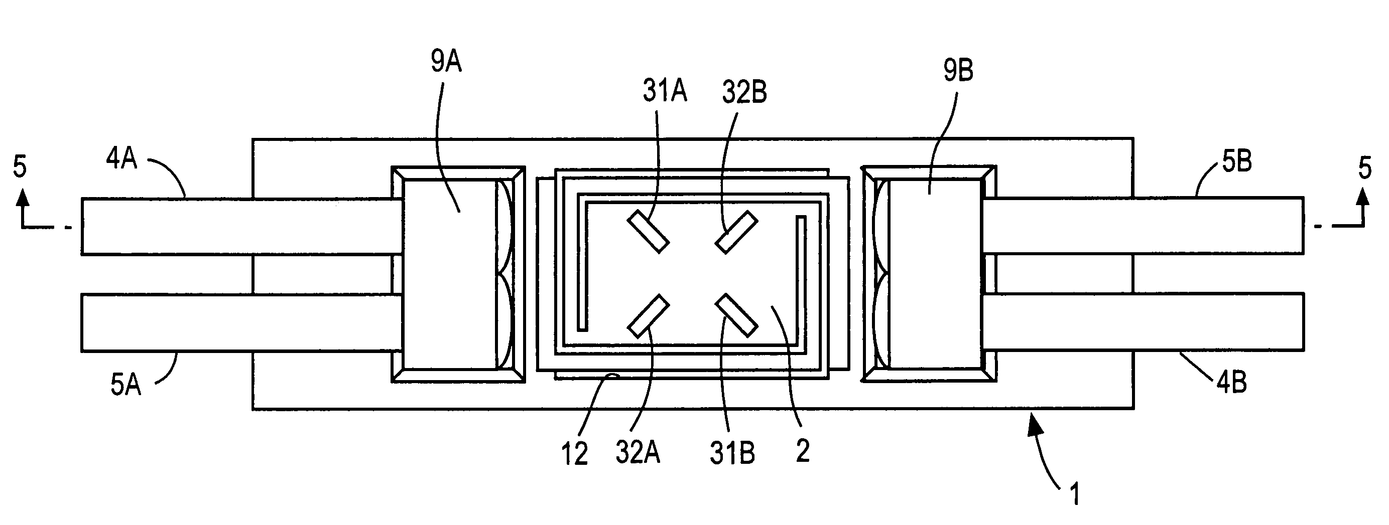
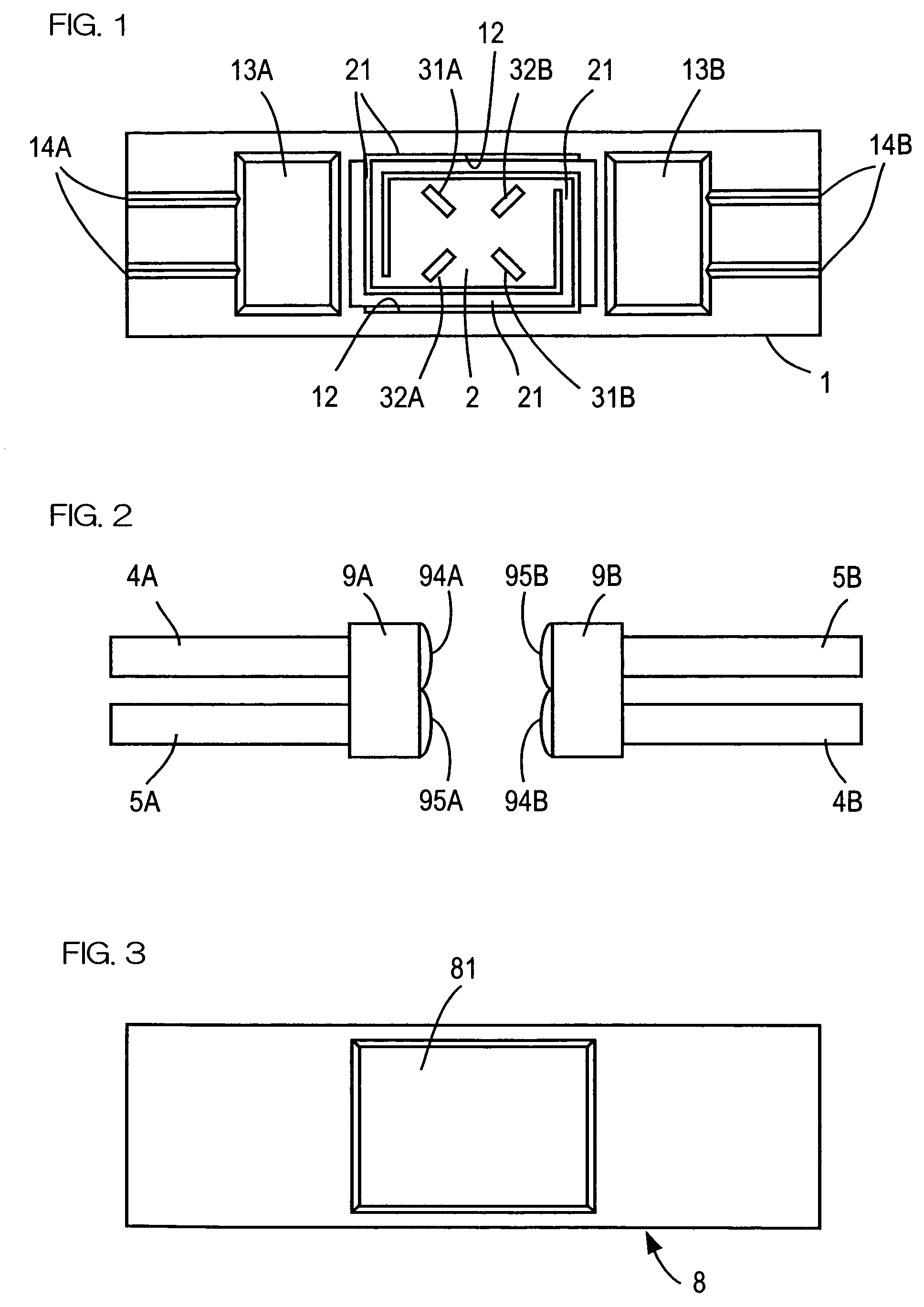
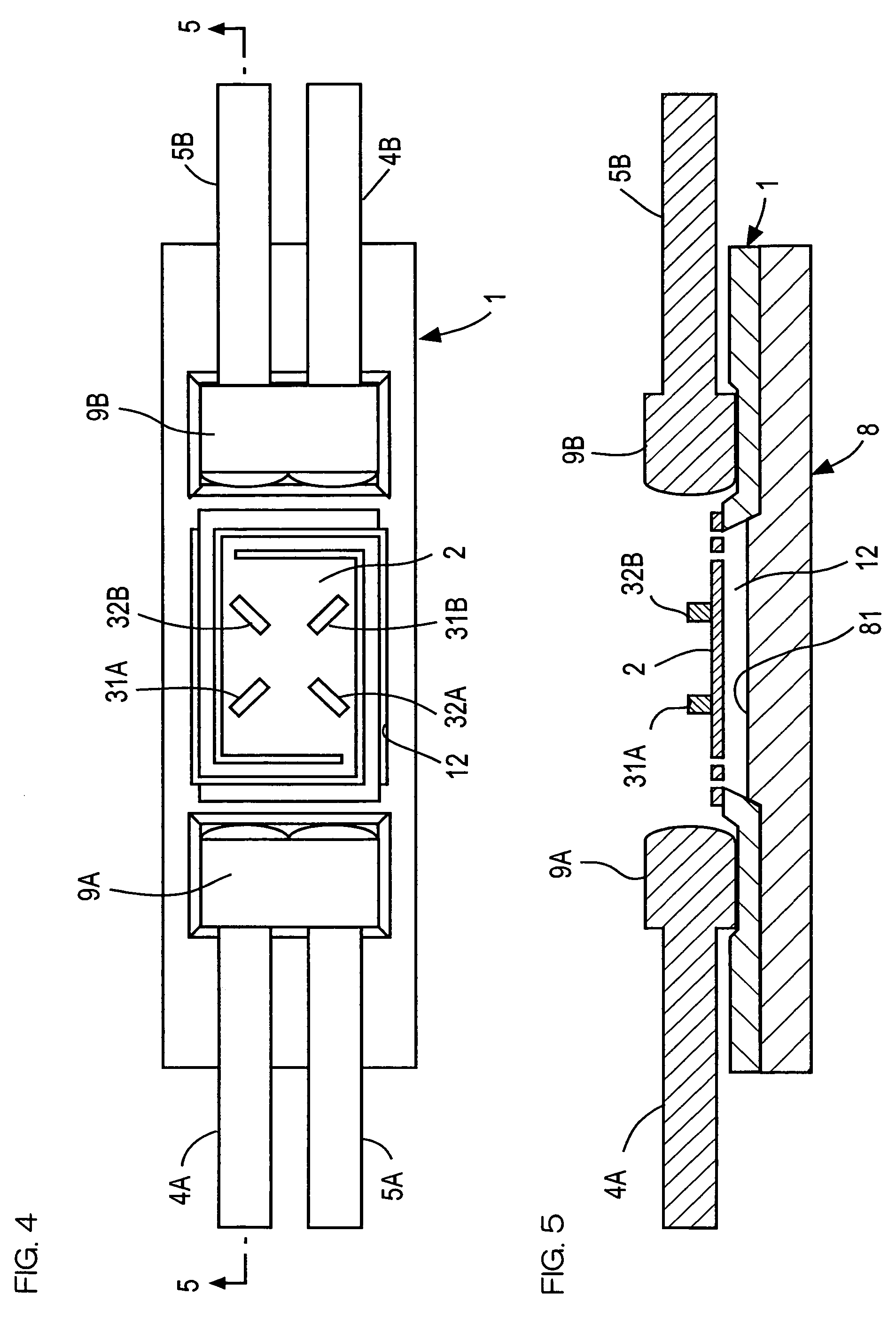
[0035]First, an example of the 2×2 optical switch to which the present invention is suitably applied will be described with reference to FIGS. 1 to 5. Further, since the 2×2 optical switch has been described in the above-stated Japanese Patent Application No. 2000-270621 (P2000-270621), the details thereof should be referred to Japanese Patent Application No. 2000-270621.

[0036]FIG. 1 is a plan view showing mainly a single crystal silicon substrate 1 having a generally rectangular shape and a movable board or plate-like electrode 2 having a...


PUM


Abstract

There is provided an optical switch that can be easily manufactured and has hardly any optical loss. A movable board-like electrode disposed in parallel with a fixed board-like electrode with a predetermined space therebetween by a flexible beam-like element, at least two mirrors fabricated on the surface of the movable board-like electrode, and at least three V-shaped grooves for fixing optical fibers are concurrently fabricated by applying an anisotropic etching to a single crystal silicon having its surface of (100) crystal face. In this case, two opposed mirrors are fabricated such that their mirror surfaces form a right angle, and two parallel V-shaped grooves are formed at positions opposed to the mirror surfaces at an angle of 45° thereto. An output side and an input side optical fibers are received and fixed in one of the two V-shaped grooves and the other groove, respectively.

Description

TECHNICAL FIELD[0001]The present invention relates to an optical switch that is used in changing the optical path of an optical signal, and in particular, it can be suitably applied to a 2×2 optical switch that is configured such that it has two output side optical fibers mounted thereto each emitting an optical signal therefrom and two input side optical fibers mounted thereto each receiving an optical signal incident thereon and that is capable of concurrently inputting optical signals emitted respectively from the two output side optical fibers into the corresponding input side optical fibers.BACKGROUND ART[0002]In a paper entitled “SELF ALIGNED VERTICAL MIRRORS AND V-GROOVES APPLIED TO A SELF-LATCHING MATRIX SWITCH FOR OPTICAL NETWORKS” presented by Philippe Helin, et al. in Thirteenth IEEE International Micro Electro Mechanical Systems Conference (MEMS-2000) held on Jan. 23 through 27, 2000 at Miyazaki, Japan, for example, a technology is described that if an orientation-depend...

Claims


Application Information

Patent Timeline
Patent Type & Authority Patents(United States)
IPC IPC(8): G02B6/26G02B6/12G02B6/35
CPCG02B6/3584G02B6/3514G02B6/3518G02B2006/12104G02B6/3546G02B6/352G02B26/08
Inventor NORIMATSU, TOSHIHIDE
Owner JAPAN AVIATION ELECTRONICS IND LTD
Features
  • R&D
  • Intellectual Property
  • Life Sciences
  • Materials
  • Tech Scout
  • Unparalleled Data Quality
  • Higher Quality Content
  • 60% Fewer Hallucinations
Learn More