Defect analyzer

a technology of defect analysis and analyzer, which is applied in the direction of instruments, nuclear elements, testing circuits, etc., can solve the problems of defect analysis often required, defects and structural causes of device failures are often hidden, and the structure complexity of today's semiconductors grows exponentially

Active Publication Date: 2006-09-05
FEI CO
View PDF29 Cites 52 Cited by
  • Summary
  • Abstract
  • Description
  • Claims
  • Application Information

AI Technical Summary

Benefits of technology

[0007]The present invention provides methods, devices, and systems for analyzing defects in an object such as a semiconductor wafer. In one embodiment, it provides a method of characterizing defects in semiconductor wafers during fabrication in a semiconductor fabrication facility. The process is partially or fully automated and can be done in the wafer fabrication facility to provide rapid feedback to process engineers to troubleshoot or improve processes.

Problems solved by technology

As device geometries continue to shrink and new materials are introduced, the structural complexity of today's semiconductors grows exponentially.
Thus, the defects and structural causes of device failure are often hidden well below the surface.
Accordingly, defect analysis often requires cross-sectioning and viewing defects on a three-dimensional basis.
This is because there are more defects that are buried and / or smaller, and in addition, chemical analysis is needed in many cases.
Unfortunately, the defect characterization provided by conventional systems (e.g., optical inspection tools) is typically inadequate.
The defect analysis process is typically slow and manual, with a technician individually deciding upon and performing each of the steps in the analysis.
The results can take too long in being returned to the fab and the delay in analysis results can result in producing more defects or shutting down production.
When a wafer is taken for detailed defect analysis, in many cases, the wafer must be discarded after it has been analyzed for fear of contamination and the like, even though only a small part of the wafer is destroyed by the analysis.
With ever increasing wafer sizes and material process complexities, such losses can result in significant financial hardships.

Method used


Image

  • Defect analyzer
  • Defect analyzer
  • Defect analyzer

Examples


Embodiment Construction

A. Overview

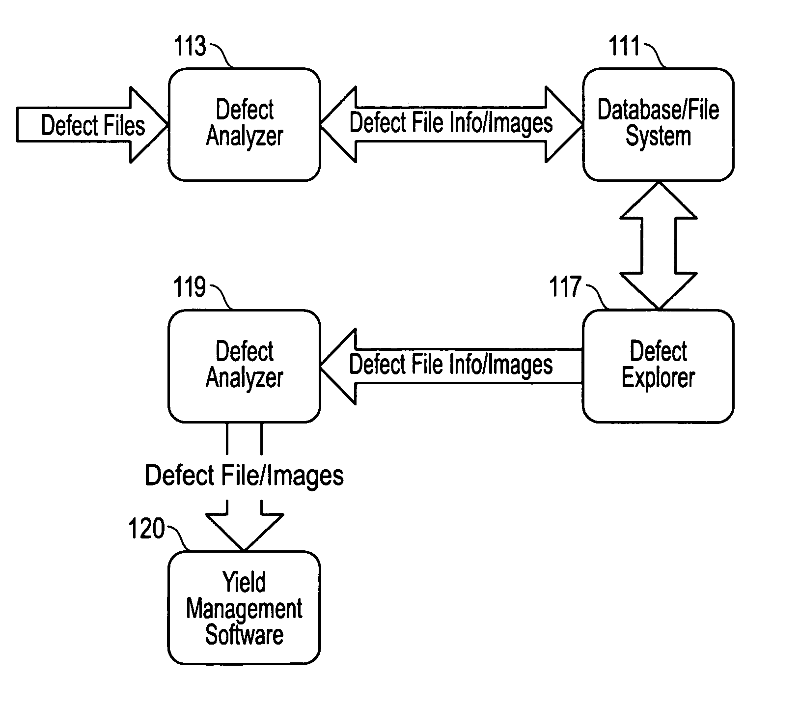
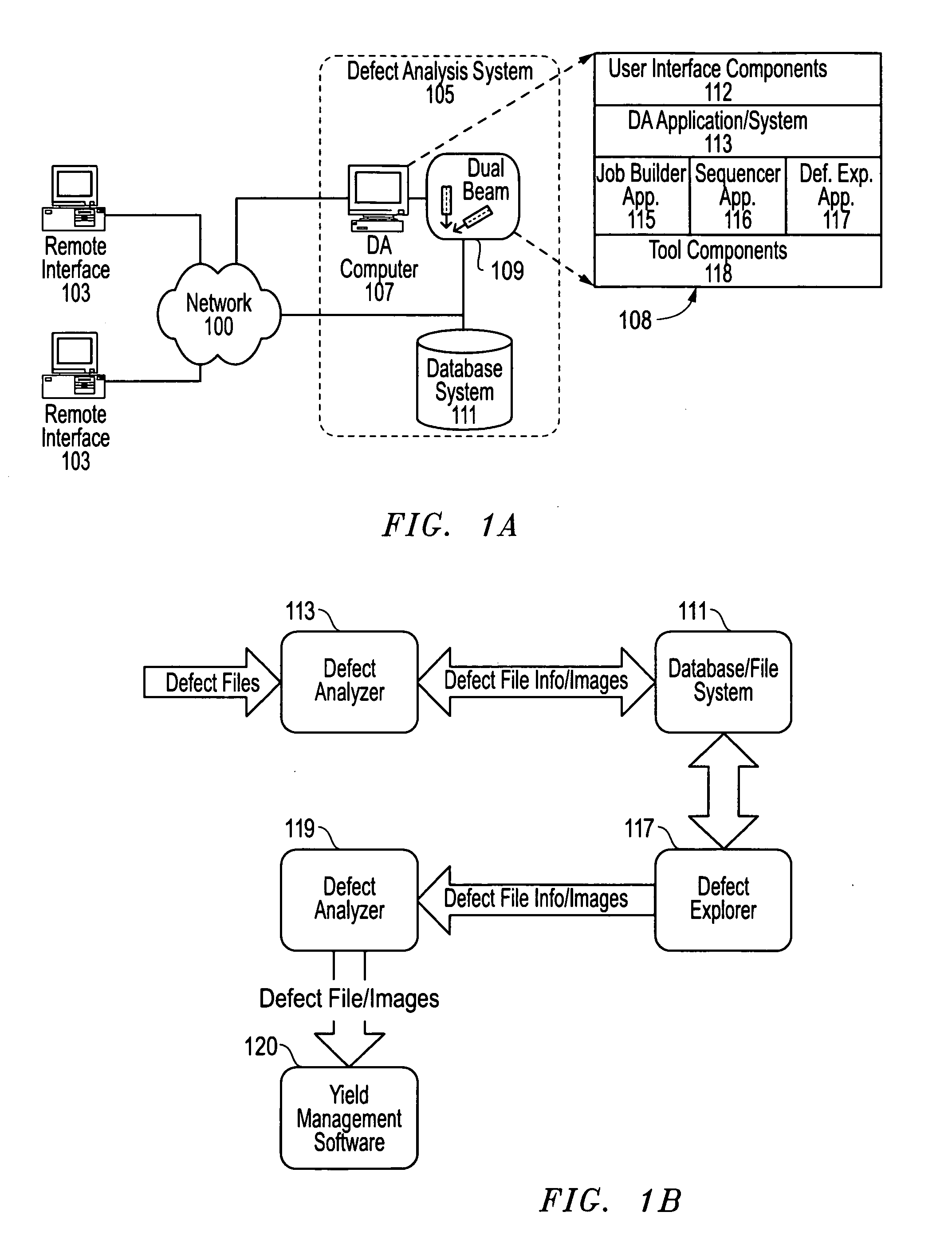
[0066]The present invention provides partly or fully automatic location and characterization of microscopic defects in items, such as integrated circuits or other structures fabricated on semiconductor wafer. The automatic characterization of the defect may include steps such as forming an image of the top surface, milling one or more cross sections, forming an image of the one or more cross-sections, performing an x-ray spectroscopy analysis (e.g., energy dispersive spectroscopy, “EDS”) to determine the type of material present on the surface or in a cross section, and storing defect characterization data. By being partly or fully automated, the invention can provide rapid feedback to process engineers. Embodiments of the invention can change the defect analysis process from a labor intensive, time consuming process performed in a laboratory to a production process that provides timely feedback to process engineers for troubleshooting or improving production.

[0067]In one...


PUM


Abstract

The present invention provides methods, devices, and systems for analyzing defects in an object such as a semiconductor wafer. In one embodiment, it provides a method of characterizing defects in semiconductor wafers during fabrication in a semiconductor fabrication facility. This method comprises the following actions. The semiconductor wafers are inspected to locate defects. Locations corresponding to the located defects are then stored in a defect file. A dual charged-particle beam system is automatically navigated to the vicinity defect location using information from the defect file. The defect is automatically identified and a charged particle beam image of the defect is then obtained. The charged particle beam image is then analyzed to characterize the defect. A recipe is then determined for further analysis of the defect. The recipe is then automatically executed to cut a portion of the defect using a charged particle beam. The position of the cut is based upon the analysis of the charged particle beam image. Ultimately, a surface exposed by the charged particle beam cut is imaged to obtain additional information about the defect.

Description

[0001]This application claims priority from U.S. Provisional Patent Application No. 60 / 425,407, filed Nov. 12, 2002.TECHNICAL FIELD OF THE INVENTION[0002]The present invention relates generally to micro-fabrication processes, and in particular, the invention relates to defect analysis systems.BACKGROUND OF THE INVENTION[0003]Engineers need to analyze defects and other failures during micro-fabrication to troubleshoot, adjust, and improve micro-fabrication processes. For example, defect analysis is useful in all aspects of semiconductor production including design verification diagnostics, production diagnostics, as well as other aspects of microcircuit research and development. As device geometries continue to shrink and new materials are introduced, the structural complexity of today's semiconductors grows exponentially. Many of the structures created with these new materials are re-entrant, penetrating back through previous layers. Thus, the defects and structural causes of device...

Claims


Application Information

Patent Timeline
Patent Type & Authority Patents(United States)
IPC IPC(8): G06F19/00H01L21/00
CPCH01J37/28H01J37/302H01J37/304H01J37/3056H01L21/67276H01L21/67253H01J2237/2485H01J2237/2817H01J2237/31745H01J2237/24592
Inventor TESHIMA, JANETPARTIN, DANIEL E.HUDSON, JAMES E.
Owner FEI CO
Why Eureka
Try Eureka