Method of acquiring an image from an optical structure having pixels with dedicated readout circuits

Inactive Publication Date: 2006-09-12
NASA
View PDF51 Cites 99 Cited by
  • Summary
  • Abstract
  • Description
  • Claims
  • Application Information

AI Technical Summary

Benefits of technology

[0013]Preferably, the output transistor is a field effect source follower transistor, the floating diffusion being connected to a gate of the source follower transistor. Preferably, the readout circuit further includes a double correlated sampling circuit having an input node connected to the output transistor. In the preferred implementation, the double correlated sampling circuit samples the floating d

Problems solved by technology

However, charge coupled device imagers suffer from a number of disadvantages.
They are particularly susceptible to radiation damage, they require good light shielding to avoid smear and they have high power dissipation for large arrays.
The difficulty is that the standard CCD process is incompatible with complementary metal oxide semiconductor (CMOS) processing

Method used


Image

  • Method of acquiring an image from an optical structure having pixels with dedicated readout circuits
  • Method of acquiring an image from an optical structure having pixels with dedicated readout circuits
  • Method of acquiring an image from an optical structure having pixels with dedicated readout circuits

Examples


Embodiment Construction

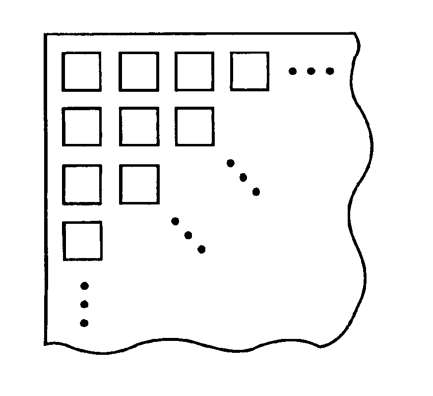
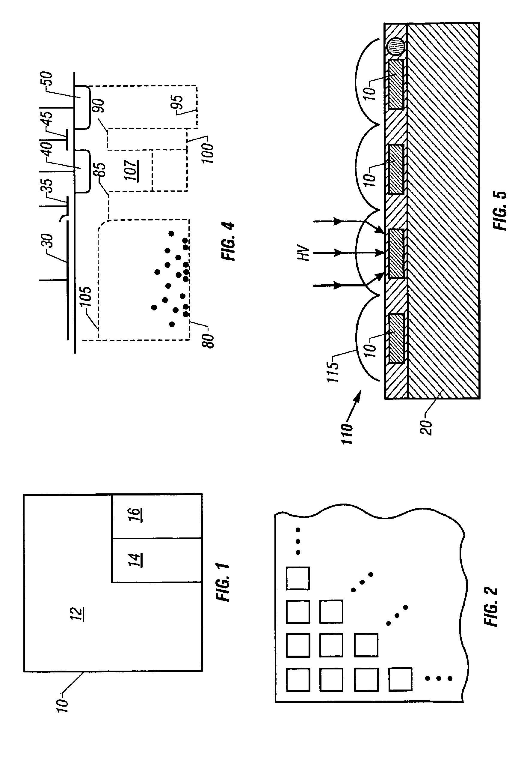
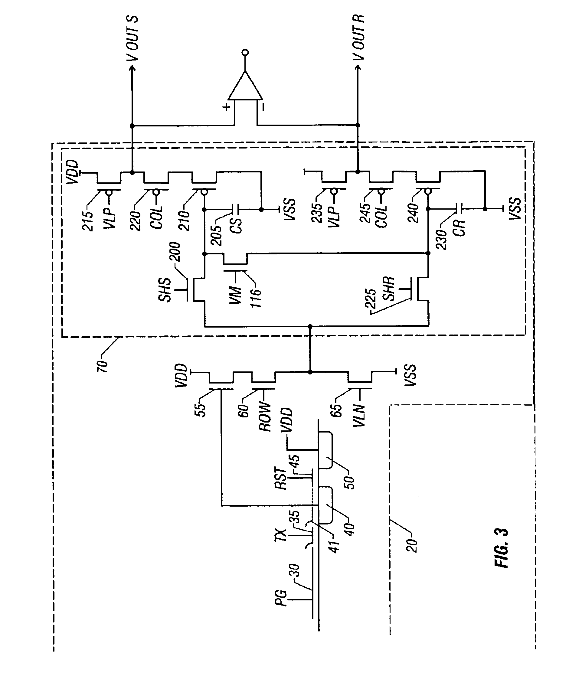
[0019]FIG. 1 is a simplied block diagram of one pixel cell 10 of a focal plane array of many such cells formed in an integrated circuit. Each cell 10 includes a photogate 12, a charge transfer section 14 adjacent the photogate 12 and a readout circuit 16 adjacent the charge transfer section 14. FIG. 2 shows a focal plane array of many cells 10 formed on a silicon substrate 20. FIG. 3 is a simplified schematic diagram of a cell 10. Referring to FIG. 3, the photogate 12 consists of a relative large photogate electrode 30 overlying the substrate 20. The charge transfer section 14 consists of a transfer gate electrode 35 adjacent the photogate electrode 30, a floating diffusion 40, a reset electrode 45 and a drain diffusion 50. The readout circuit 16 consists of a source follower field effect transistor (FET) 55, a row select FET 60, a load FET 65 and a correlated double sampling circuit 70.

[0020]Referring to the surface potential diagram of FIG. 4, the photogate electrode 30 is held by...


PUM


Abstract

An imaging device formed as a monolithic complementary metal oxide semiconductor integrated circuit in an industry standard complementary metal oxide semiconductor process, the integrated circuit including a focal plane array of pixel cells, each one of the cells including a photogate overlying the substrate for accumulating photo-generated charge in an underlying portion of the substrate, a readout circuit including at least an output field effect transistor formed in the substrate, and a charge coupled device section formed on the substrate adjacent the photogate having a sensing node connected to the output transistor and at least one charge coupled device stage for transferring charge from the underlying portion of the substrate to the sensing node.

Description

CROSS-REFERENCE TO RELATED APPLICATIONS[0001]This application is a divisional of U.S. application Ser. No. 10 / 388,250, filed on Mar. 12, 2003 now U.S. Pat. No. 6,744,068, which is a divisional of U.S. application Ser. No. 09 / 604,846 filed on Jun. 27, 2000 now U.S. Pat. No. 6,555,842 and U.S. application Ser. No. 08 / 558,521 filed Nov. 16, 1995, now U.S. Pat. No. 6,101,232 issued Aug. 8, 2000, and U.S. application Ser. No. 08 / 188,032 filed Jan. 28, 1994, now U.S. Pat. No. 5,471,515 issued Nov. 28, 1995.ORIGIN OF THE INVENTION[0002]The invention described herein was made in the performance of work under a NASA contract, and is subject to the provisions of Public Law 96-517 (35 USC 202) in which the Contractor has elected to retain title.BACKGROUND OF THE INVENTION[0003]1. Technical Field[0004]The invention is related to semiconductor imaging devices and in particular to a silicon imaging device which can be fabricated using a standard CMOS process.[0005]2. Background Art[0006]There are...

Claims


Application Information

Patent Timeline
IPC IPC(8): H01L29/04G11C19/28H01L27/146H01L27/148H01L31/0216H01L31/0232H04N5/345H04N5/353H04N5/357H04N5/361H04N5/363H04N5/365H04N5/369H04N5/374H04N5/3745H04N5/376H04N5/378H04N9/04
CPCG11C19/282H01L27/14601H01L27/14621H01L27/14627H01L27/14645H01L27/14656H01L27/14843H01L27/1485H01L27/14887H04N3/155H04N3/1562H04N3/1568H04N5/3575H04N5/361H04N5/363H04N5/3658H04N5/374H04N5/3745H04N5/37452H04N5/378G11C19/285H04N9/045H01L31/02162H01L31/0232H01L27/14603H04N25/616H04N25/65H04N25/677H04N25/63H04N25/771H04N25/70H04N25/77H04N23/10H04N25/76H04N25/75
Inventor FOSSUM, ERIC R.MENDIS, SUNETRAKEMENY, SABRINA E.
Owner NASA
Why Eureka
Try Eureka