CMOS type image sensor module having transparent polymeric encapsulation material
Active Publication Date: 2006-09-12
SAMSUNG ELECTRONICS CO LTD
View PDF11 Cites 21 Cited by
Summary
Abstract
Description
Claims
Application Information
AI Technical Summary
This helps you quickly interpret patents by identifying the three key elements:
Problems solved by technology
Method used
Benefits of technology
Benefits of technology
[0011]An object of the present invention is to provide a CMOS type of image sensor module that can be produced using a relatively simple process.
[0012]Another object of the present invention is to provide a compact CMOS type of image sensor module.
[0013]Still another object of the present invention is to provide a CMOS type of image sensor module that is easy to mass produce.
Problems solved by technology
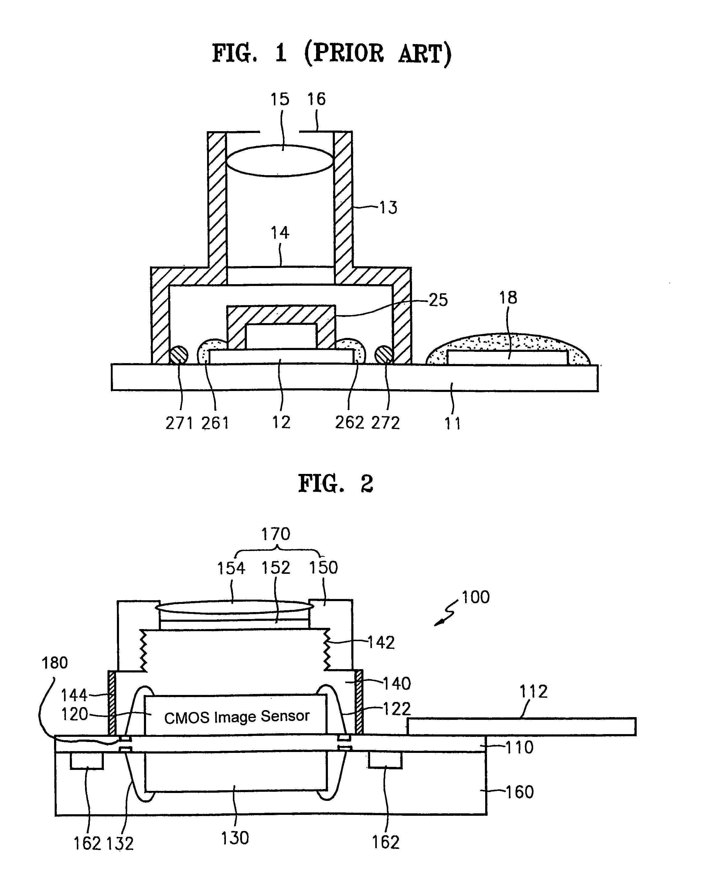
First, the manufacturing of the CMOS type of image sensor module is a complicated process entailing a high production cost because it involves creating a seal between the lens kit 13 and the substrate 11. Moreover, the image sensoring semiconductor chip 12 and the digital signal processing semiconductor chip 18 are molded to the substrate 11 through separate processes.
Second, the difficulties and complexity of the manufacturing process, especially when adapted for mass production of the CMOS type of image sensor module, lead to frequent manufacturing defects. That is, the prior art CMOS type of image sensor module is manufactured with a relatively low productivity.
Third, the prior art CMOS type of image sensor module is relatively large because the image sensoring semiconductor chip and the digital signal processing semiconductor chip are mounted to the substrate horizontally as spaced laterally from each other.
Method used
Image
Click on the blue label to locate the original text in one second.
Reading with bidirectional positioning of images and text.
Examples
first embodiment
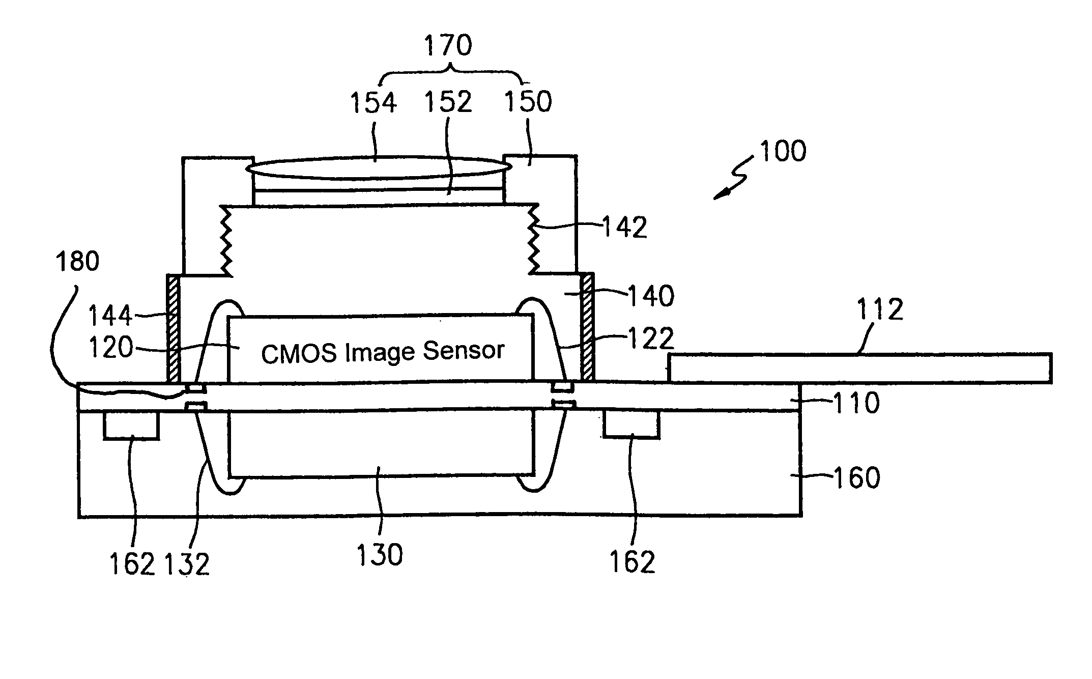
[0026]Referring to FIG. 2, CMOS type of image sensor module 100 according to the present invention includes a substrate 110 having a circuit pattern 180 to which a chip can be wire bonded at either side thereof, a first semiconductor chip (image sensing chip having a CMOS type of image sensor) 120 mounted on an upper portion of the substrate 110 and wire-bonded to the circuit pattern thereof, a second semiconductor chip (digital signal processing chip) 130 mounted on a lower portion of the substrate 110 and wire-bonded to the circuit pattern thereof, and a sealing resin unit 140 of transparent polymeric encapsulation material formed on the surface of the substrate 110 by injection molding and in which the first semiconductor chip 120 is sealed.
[0027]The CMOS type of image sensor module 100 further includes an epoxy molding compound 160 on the lower portion of the substrate 110 and in which a passive device 162 and the second semiconductor chip 130 are sealed, protective material 144...
third embodiment
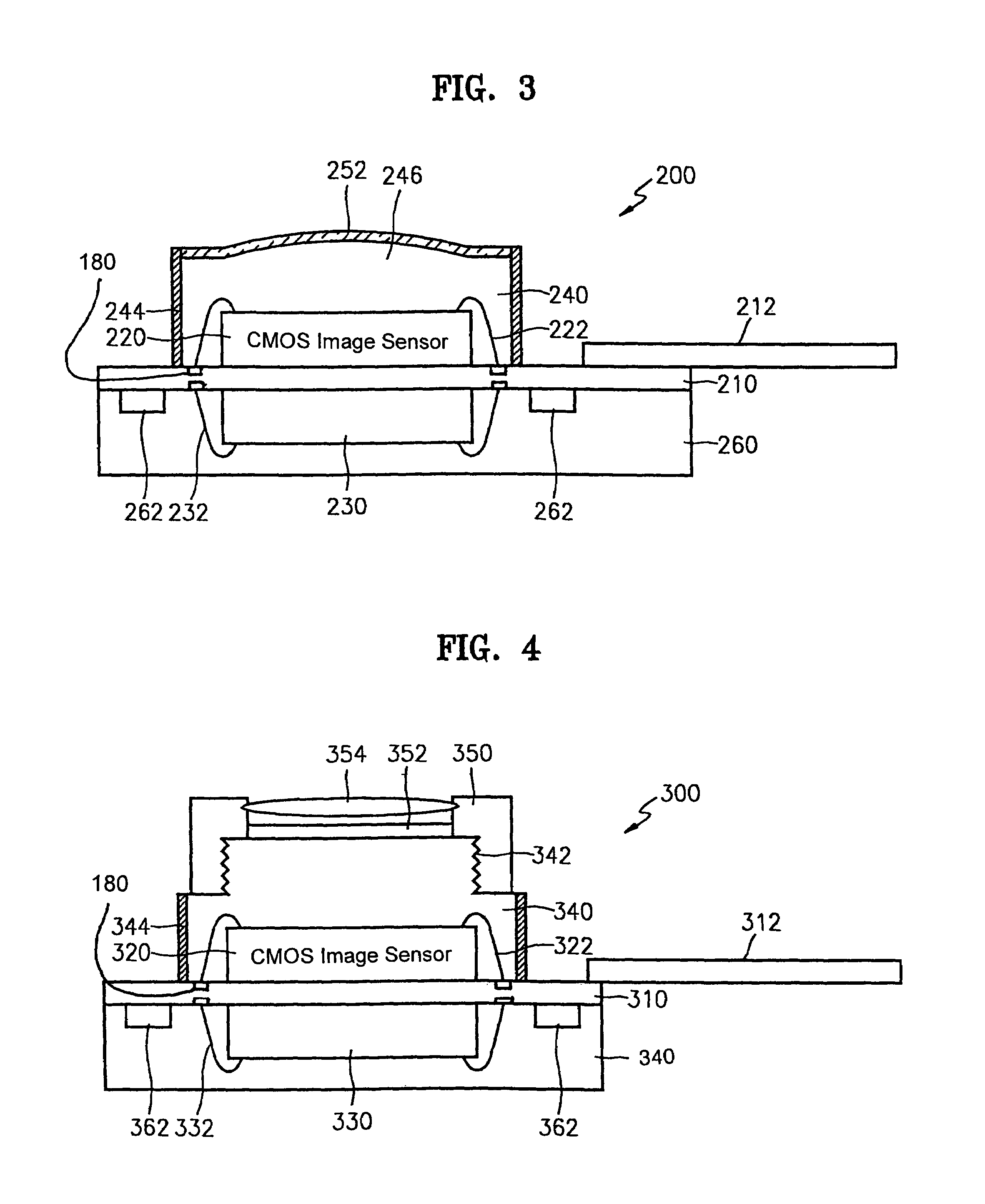
[0038]a CMOS type of image sensor module according to the present invention will now be described with reference to FIG. 4.
[0039]In this embodiment, a sealing resin unit 340 is formed on both the upper and lower portion of a substrate 310, i.e., an epoxy compound is not molded to the lower portion of the substrate 310. The remaining parts are identical to those of the embodiment of FIG. 2. For instance, the sealing resin unit 340 has a screw thread 342, and a lens kit is threaded to the sealing resin unit 342. The lens kit includes a lens housing 350, an infrared filter 352, and an optical lens 354. Reference numerals 322, 332 designate bonding wires, 362 a passive device, and 312 a flexible printed circuit board (FPCB).
fourth embodiment
[0040]a CMOS type of image sensor module according to the present invention will now be described with reference to FIG. 5.
[0041]This embodiment is the same as the third embodiment in that a sealing resin unit 440 is formed on both the upper and lower portions of the substrate 410, i.e., an epoxy compound is not molded to the lower portion of the substrate 410. In this embodiment, though, like the second embodiment of FIG. 3, an optical lens 446 is formed by the upper portion of the sealing resin unit 440, and the plastic lens 446 is coated with an infrared filter 452. Reference numerals 422, 432 designate bonding wires, 462 a passive device, and 412 a flexible printed circuit board (FPCB).
[0042]Methods of manufacturing CMOS type of image sensor modules 300 and 400 according to the present invention will be described below.
[0043]First, a substrate 310, 410 including a circuit pattern at both sides thereof is prepared. The doubled-sided substrate 310, 410 is similar to that of a ball...
PUM
Abstract
A CMOS type of image sensor module for use in a mobile camera or a PC camera includes an image sensoring semiconductorchip encapsulated in a transparent block of polymeric material on a substrate having a circuit to which the ship is connected. The image sensoring semiconductorchip is disposed on an upper surface of the substrate as spaced vertically from a digital signalprocessing second semiconductorchip mounted on a lower surface of the substrate. The transparent polymeric encapsulation material constitutes a sealing resin unit. The digital signalprocessing second semiconductor chip may also be encapsulated by the sealing resin unit. The sealing transfer unit can be formed by injection and / or transfer molding. The forming of the sealing resin unit by a single molding process keeps production costs low.
Description
BACKGROUND OF THE INVENTION[0001]1. Field of the Invention[0002]The present invention relates to an image pick up device for use in a mobile camera or the like. More particularly, the present invention relates to a CMOS type image sensor module including a semiconductor chip having a CMOS-based sensor for picking up an image, and a built-in digital signalprocessingsemiconductor chip.[0003]2. Description of the Related Art[0004]A known image sensor module of a camera is a multi-chip device that includes an image sensoring semiconductor chip and a digital signal processing semiconductor chip. The image sensoring semiconductor chip collects optical images, and the digital signal processing semiconductor chip converts the optical images into electrical signals. Based on the particular type of semiconductor used, the image sensor modules are classified as a charge coupled device (CCD) or a complementary metaloxide semiconductor (CMOS) device.[0005]A CMOS type of image sensor module is...
Claims
Application Information
Patent Timeline
Application Date:The date an application was filed.
Publication Date:The date a patent or application was officially published.
First Publication Date:The earliest publication date of a patent with the same application number.
Issue Date:Publication date of the patent grant document.
PCT Entry Date:The Entry date of PCT National Phase.
Estimated Expiry Date:The statutory expiry date of a patent right according to the Patent Law, and it is the longest term of protection that the patent right can achieve without the termination of the patent right due to other reasons(Term extension factor has been taken into account ).
Invalid Date:Actual expiry date is based on effective date or publication date of legal transaction data of invalid patent.

