Semiconductor integrated circuit

a technology of integrated circuits and semiconductors, applied in the field of semiconductor integrated circuits, can solve the problems of increasing emi noise in the schmitt circuit contrary, steep and complicated waveform shaping section power-source current ivdd flowing through the waveform shaping section, and deteriorating emi characteristics in the high frequency region, so as to reduce the emi noise produced

Inactive Publication Date: 2006-09-12
RENESAS ELECTRONICS CORP
View PDF16 Cites 0 Cited by
  • Summary
  • Abstract
  • Description
  • Claims
  • Application Information

AI Technical Summary

Benefits of technology

[0018]An object of the invention is to provide a semiconductor integrated circuit reducing EMI noise produced by an oscillator by dividing the oscillator into an oscillating section and a waveform shaping section.

Problems solved by technology

Therefore, the reduction of noise caused by the oscillator is one of the challenges for the reduction of EMI noise.
Therefore, the waveform-shaping section power-source current Ivdd flowing through the waveform shaping section becomes steep and complicated, as shown in the waveform-shaping section power-source current Ivdd of FIG. 3, and thus its spectra spreads to the high frequency region.
However, the conventional prior art has a problem that the insertion of the Schmitt circuit contrary increases EMI noise due to the following reasons.
In other words, there is a problem in which the insertion of the Schmitt circuit deteriorates EMI characteristics in the high frequency region because of an increased through-current induced by the adding of transistor element itself and the complicated current characteristics of the Schmitt circuit.
However, in the case of the oscillator, there is also a problem that insertion of a pass capacitor in the vicinity of the oscillator, is not so effective for the reduction of noise produced by the waveform shaping section including the Schmitt circuit since the capacitor is mostly used for charging and discharging of the feedback inverter within the oscillating section, as shown for the oscillation power-source current Ivddosc in FIG. 3.

Method used


Image

  • Semiconductor integrated circuit
  • Semiconductor integrated circuit
  • Semiconductor integrated circuit

Examples


first embodiment

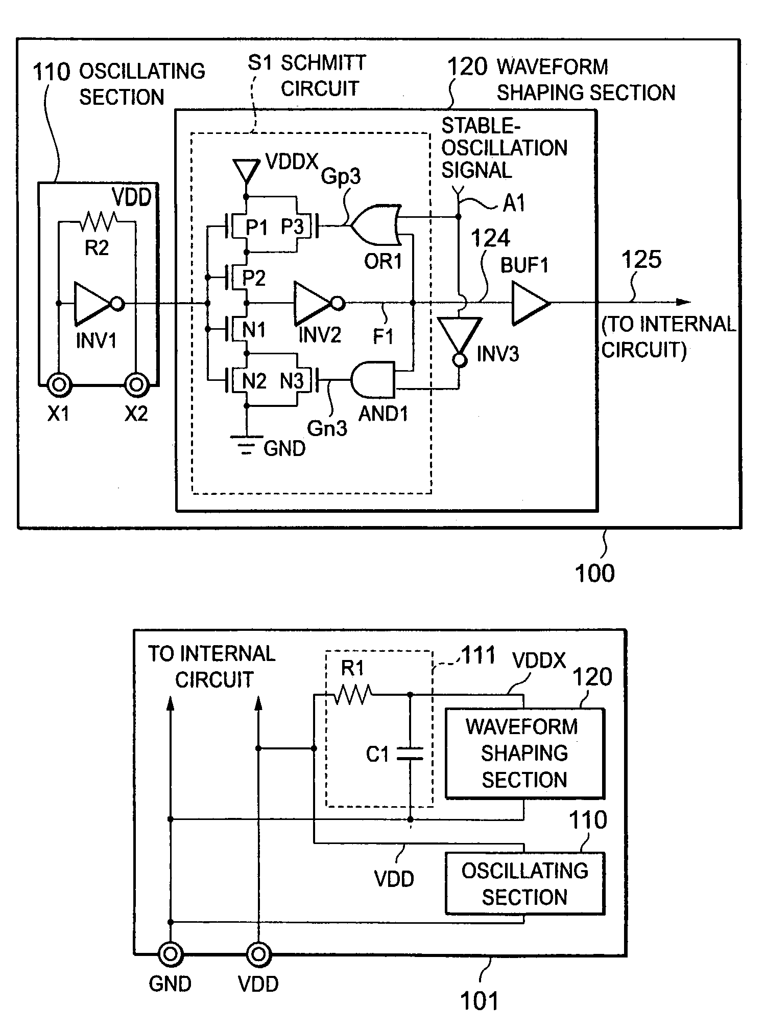
[0038]FIG. 4A is a block diagram for showing a detailed configuration of a semiconductor integrated circuit according to the invention, and FIG. 4B is the configuration of the supply of power thereto.

[0039]Referring to FIG. 4A, in a semiconductor integrated circuit 100 according to the first embodiment of the invention, the built-in oscillation circuit comprises an oscillating section 110 consisting of a feedback inverter INV1 and a feedback resistor R2, and a waveform shaping section 120.

[0040]Further, the supplies of power are separately provided to the oscillating section 110 and waveform shaping section 120, respectively. That is, referring to FIG. 4B, the supply of power to the waveform shaping section 120 is provided through a low pass filter 111 comprised of a resistor R1 and a capacitor C1, wherein a high potential power source VDD is supplied to the waveform shaping section as a high potential power source VDDX.

[0041]Also, transistor element P3 and N3 of a Schmitt circuit S...

second embodiment

[0049]In the semiconductor integrated circuit according to the invention, when the stable-oscillation signal A2 becomes HIGH, the input of the Schmitt circuit S1 is fixed to GND, thereby operating to eliminate the through-current flowing through the Schmitt circuit S1. At this time, if the constituent elements of an inverter INV4 are in advance designed to be small in the current-driving ability, the through-current flowing through the whole of the waveform shaping section can be further decreased, and therefore it is possible to substantially suppress the production of high frequency noise.

[0050]Next, a semiconductor integrated circuit according to a third embodiment of the invention will be described. FIG. 8 is a block diagram for showing a semiconductor integrated circuit according to a third embodiment of the invention.

[0051]After the semiconductor integrated circuit according to the first embodiment of the invention reaches to stable oscillation, it eliminates the hysteresis ch...

third embodiment

[0052]In a the semiconductor integrated circuit 500 according to the invention, after the stable-oscillation signal A3 becomes HIGH, the transistor elements P7 and N7 each become OFF, but the transistor elements P6 and N6 keep their hysteresis characteristics themselves because the output of an INV6 continues inputting thereto. However, because the transistor elements P7 and N7 become OFF, the widths of hysteresis of the transistor elements P6 and N6 are narrower than those when the stable-oscillation signal A3 is LOW, but the production of high frequency noise can be suppressed by the corresponding amount.

[0053]In general, after the oscillation becomes stable, the effect of external noise input via the oscillating section 110 is decreased because the output of the feedback inverter has an inductance component. Therefore, by suppressing to a required minimum the hysteresis width after the oscillation becomes stable, it possible to keep EMS characteristics while suppressing the produ...


PUM


Abstract

An oscillating section 110 comprised of feedback inverter INV1 and a feedback resistor R2, and a waveform shaping section 120 including a Schmitt circuit S1 of which transistors P3 and N3 respectively receive, as gate control signals, signals Gp3 and Gn3 generated by a stable-oscillation signal A1 and logic elements AND1, OR1 and INV3, respectively, and the supply of power to the waveform shaping section 120 is performed through a low pass filter 111 comprised of a resistor R1 and a capacitor C1 and thus a high potential power source VDD is supplied to the waveform shaping section 120 as a high potential power source VDDX.

Description

BACKGROUND OF THE INVENTION[0001]1. Field of the Invention[0002]The invention relates to semiconductor integrated circuits, and more particularly to a semiconductor integrated circuit containing an oscillator and reducing Electro-Magnetic interference (hereinafter, abbreviated to EMI) noise produced by the oscillator.[0003]2. Description of the Prior Art[0004]As is well known, smaller sets of electrical equipment are introduced because of the recent technical trend of module integration that is proceeding in the automotive electrical equipment industry. This leads to an increasing demand for reducing EMI noise in FM band / keyless band (Rf band) of the individual semiconductor integrated circuits (semiconductor devices) installed in the set, which is also well known.[0005]It is also well known that a variety of factors are responsible for EMI noise of such semiconductor integrated circuits.[0006]EMI noise caused by an oscillator integrated in the above described semiconductor integrat...

Claims


Application Information

Patent Timeline
IPC IPC(8): H03B1/00H03B5/02H03B5/32H03K3/013H03K3/03
CPCH03K3/0307H03K3/013H03K5/08
Inventor MATSUSHITA, RUMI
Owner RENESAS ELECTRONICS CORP
Why Eureka
Try Eureka