
Manufacturing test for a fault tolerant magnetoresistive solid-state storage device

a solid-state storage and fault-tolerant technology, applied in the direction of digital storage, error detection/correction, instruments, etc., can solve the problems of inability to manufacture mram devices that are subject to limitations, inability to accept stored data loss, and low manufacturing yield of commercially acceptable mram devices

Inactive Publication Date: 2006-09-12
SAMSUNG ELECTRONICS CO LTD
View PDF38 Cites 4 Cited by
  • Summary
  • Abstract
  • Description
  • Claims
  • Application Information

AI Technical Summary

Benefits of technology

[0004]Recently, a magnetoresistive storage device has been developed as a new type of non-volatile solid-state storage device (see, for example, EP-A-0918334 Hewlett-Packard). The magnetoresistive solid-state storage device is also known as a magnetic random access memory (MRAM) device. MRAM devices have relatively low power consumption and relatively fast access times, particularly for data write operations, which renders MRAM devices ideally suitable for both short term and long term storage applications.
[0005]A problem arises in that MRAM devices are subject to physical failure, which can result in an unacceptable loss of stored data. Currently available manufacturing techniques for MRAM devices are subject to limitations and as a result manufacturing yields of commercially acceptable MRAM devices are relatively low. Although better manufacturing techniques are being developed, these tend to increase manufacturing complexity and cost. Hence, it is desired to apply lower cost manufacturing techniques whilst increasing device yield. Further, it is desired to increase cell density formed on a substrate such as silicon, but as the density increases manufacturing tolerances become increasingly difficult to control, again leading to higher failure rates and lower device yields. Since the MRAM devices are at a relatively early stage in development, it is desired to allow large scale manufacturing of commercially acceptable devices, whilst tolerating the limitations of current manufacturing techniques.BRIEF SUMMARY OF THE INVENTION

Problems solved by technology

A problem arises in that MRAM devices are subject to physical failure, which can result in an unacceptable loss of stored data.
Currently available manufacturing techniques for MRAM devices are subject to limitations and as a result manufacturing yields of commercially acceptable MRAM devices are relatively low.
Although better manufacturing techniques are being developed, these tend to increase manufacturing complexity and cost.
Further, it is desired to increase cell density formed on a substrate such as silicon, but as the density increases manufacturing tolerances become increasingly difficult to control, again leading to higher failure rates and lower device yields.

Method used


Image

  • Manufacturing test for a fault tolerant magnetoresistive solid-state storage device
  • Manufacturing test for a fault tolerant magnetoresistive solid-state storage device
  • Manufacturing test for a fault tolerant magnetoresistive solid-state storage device

Examples


Embodiment Construction

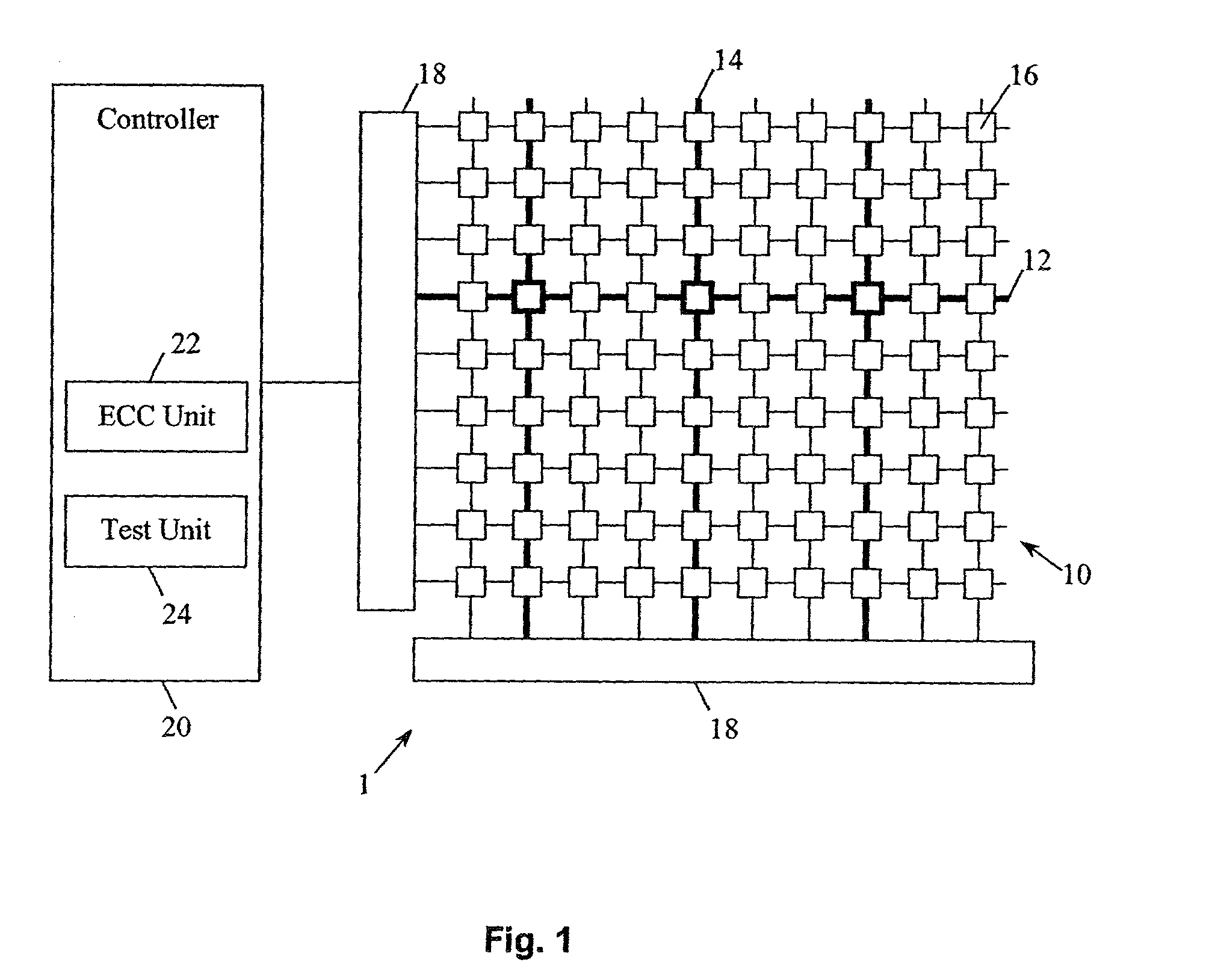
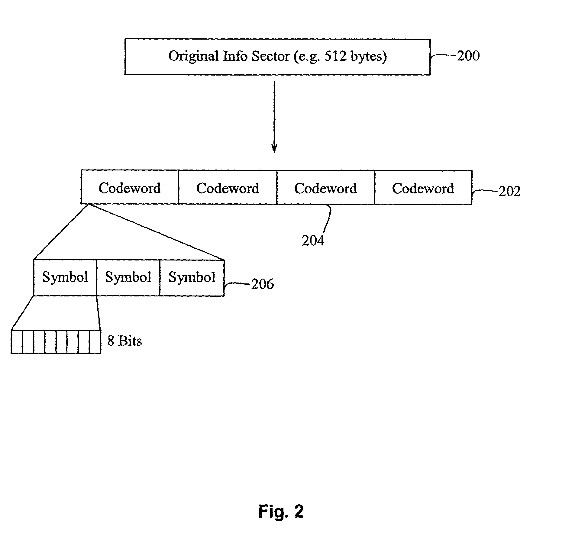
[0020]To assist a complete understanding of the present invention, an MRAM device will first be described with reference to FIG. 1, including a description of the failure mechanisms found in example forms of MRAM devices. A preferred logical data structure will then be described with reference to FIG. 2, employed when storing ECC encoded data in the device in use. A storage cell will be described in more detail referring to FIG. 3. A preferred method for reading ECC encoded data from an MRAM device in use will be described with reference to FIG. 4. Finally, the preferred method for testing an MRAM device will be described with reference to FIG. 5.

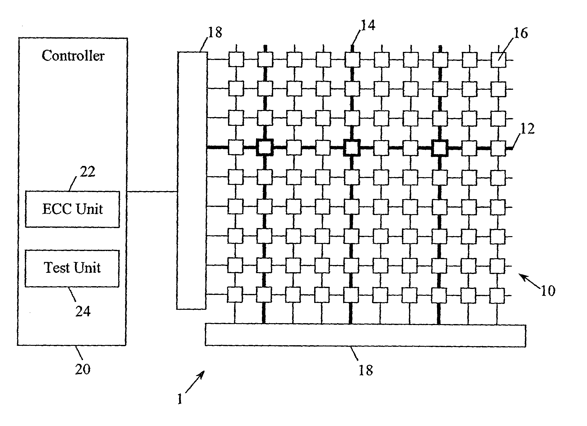
[0021]FIG. 1 shows a simplified magnetoresistive solid-state storage device 1 comprising an array 10 of storage cells 16. The array 10 is coupled to a controller 20 which, amongst other control elements, includes an ECC coding and decoding unit 22 and a test unit 24. The controller 20 and the array 10 can be formed on a single substrate, or...


PUM


Abstract

A fault-tolerant magnetoresistive solid-state storage device (MRAM) in use performs error correction coding and decoding of stored information, to tolerate physical failures. At manufacture, the device is tested to confirm that each set of storage cells is suitable for storing ECC encoded data. The test comprises identifying failed cells where the failures will be visible in use for the generation of erasure information used in ECC decoding, by comparing parametric values obtained from the cells against one or more failure ranges, and includes performing a write-read-compare operation with test data to identify failed cells which will be hidden for the generation of erasure information in use. A failure count is formed based on both the visible failures and the hidden failures, to determine that the set of cells is suitable for storing ECC encoded data. The failure count is weighted, with hidden failures having a greater weighting than visible failures.

Description

CROSS REFERENCE TO RELATED APPLICATIONS[0001]This application is a continuation-in-part of application No. 09 / 915,179, filed on Jul. 25, 2001 now abandoned.[0002]The present invention relates in general to a magnetoresistive solid-state storage device and to a method for testing a magnetoresistive solid-state storage device. In particular, but not exclusively, the invention relates to a method for testing a magnetoresistive solid-state storage device that in use will employ error correction coding (ECC).[0003]A typical solid-state storage device comprises one or more arrays of storage cells for storing data. Existing semiconductor technologies provide volatile solid-state storage devices suitable for relatively short term storage of data, such as dynamic random access memory (DRAM), or devices for relatively longer term storage of data such as static random access memory (SRAM) or non-volatile flash and EEPROM devices. However, many other technologies are known or are being develope...

Claims


Application Information

Patent Timeline
Patent Type & Authority Patents(United States)
IPC IPC(8): G11C29/00G06F12/16G11C11/15G11C29/42
CPCG11C11/16G06F11/1048G11C29/44G11C29/42
Inventor JEDWAB, JONATHANDAVIS, JAMES ANDREWPATERSON, KENNETH GRAHAMSEROUSSI, GADIEL
Owner SAMSUNG ELECTRONICS CO LTD
Learn More