Amplifier circuit with a switching device to provide a wide dynamic output range

a switching device and amplifier circuit technology, applied in the field of amplifying signals, can solve the problems of inability to operate at high speed, defect in final inspection or failure of photodiodes, and wide spread, so as to avoid any impact on circuit shot noise and magnify the output current. the effect of the dynamic rang

Inactive Publication Date: 2006-09-19
APPLIED MATERIALS INC
View PDF4 Cites 19 Cited by
  • Summary
  • Abstract
  • Description
  • Claims
  • Application Information

AI Technical Summary

Benefits of technology

[0023]In such a photomultiplier tube configuration the dynamic range of the output current can be magnified whilst avoiding any impact on the circuit's shot noise. Furthermore, the output signal can be dynamically controlled and / or selected due to an inherent provision of gain selection with the choice of dynode outputs.

Problems solved by technology

In particular, the increased use of semiconductor technology has resulted from a widespread, unappeasable need by business (as well as individuals) for better, smaller, faster and more reliable electronic goods.
This is preferable to completing the whole wafer manufacturing process, only to find that a defect exists in a final inspection or by failure during use.
For signals where light intensity is low, photodiodes cannot operate at high speed, due to their relatively high noise level of the diode, and the small currents generated by the low light energy signals.
Even though photodiodes have excellent dynamic range, their output is proportional to the optical signal, so in practice their useful dynamic range is quickly limited by subsequent electronics.
However, for the vast majority of photosensitive applications, phototubes do not have the internal amplification required to provide acceptable sensitivity and performance.
However, the large voltages involved make it difficult to change the gain quickly, due to parasitic capacitances and the large resistor values needed to limit power dissipation in the bias string.
Hence, the use of known photomultiplier tubes in an optical inspection arrangement for wafers and semiconductors has a number of significant disadvantages, not least the limited dynamic range associated with the signal amplification process and fixed gain associated with the input to output signal.

Method used


Image

  • Amplifier circuit with a switching device to provide a wide dynamic output range
  • Amplifier circuit with a switching device to provide a wide dynamic output range
  • Amplifier circuit with a switching device to provide a wide dynamic output range

Examples


Embodiment Construction

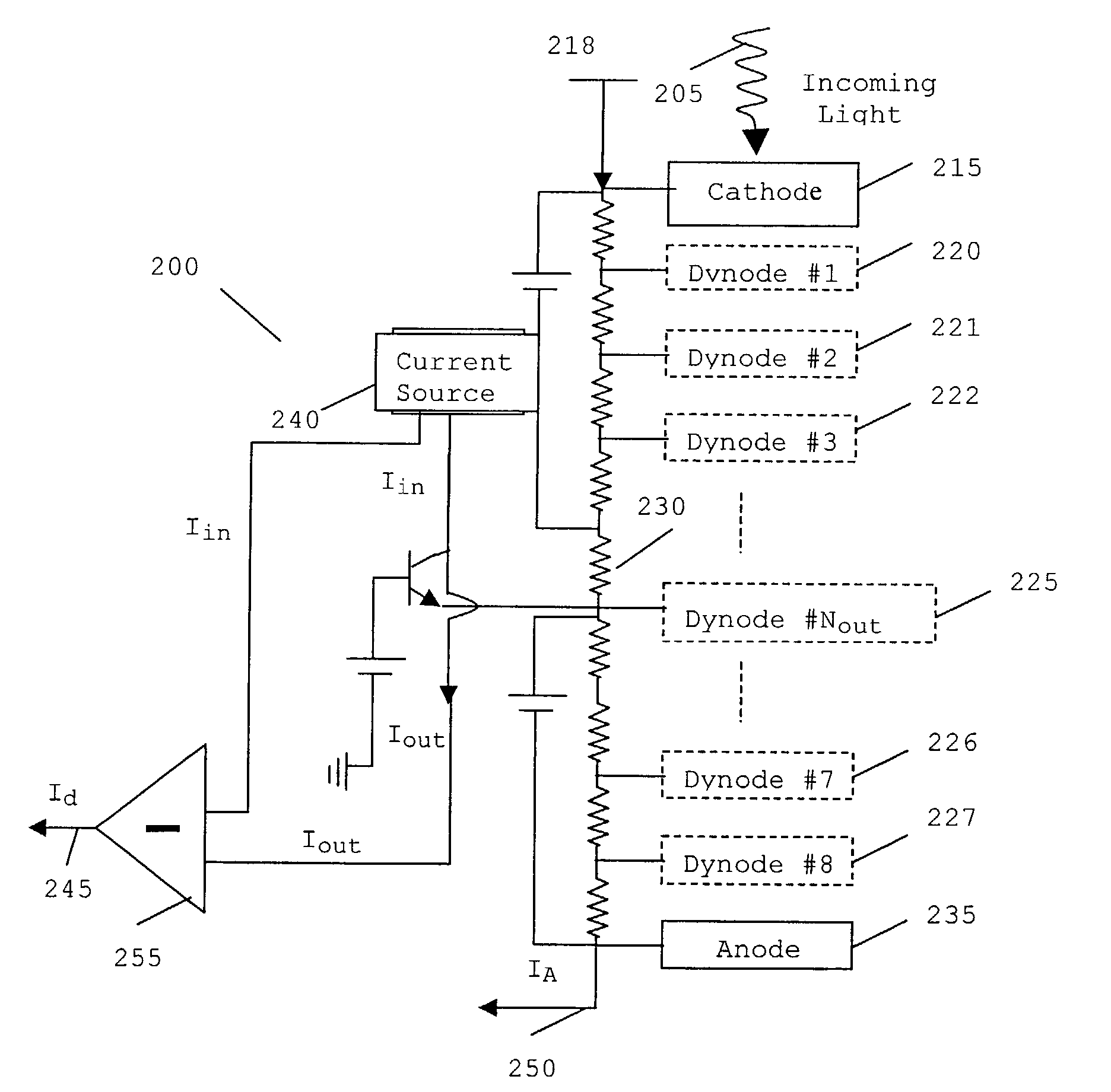
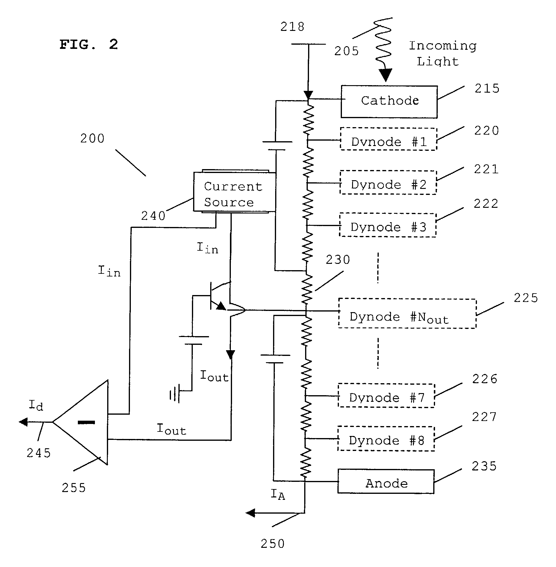
[0033]In summary, the present invention realizes optical signal detection from one or more PMT dynode outputs, in contrast to the conventional process of realizing signal detection only at the anode output.

[0034]Referring now to FIG. 2, incoming light 205 is directed onto a photocathode 215, which is operably coupled to an anode 235 by a series of dynodes 220–227. A large negative voltage 218 is applied to the cathode 215, and the potential is divided up across the dynodes 220–227 by the voltage-divider resistor chain 230. In accordance with the preferred embodiment of the present invention, the voltage-divider resistor chain 230 may or may not apply a linear potential drop, i.e. the resistor chain may comprise a variety of resistor values.

[0035]When light 205 of sufficient energy strikes the photocathode 215, the photocathode emits photoelectrons into the vacuum due to the photoelectric effect, in the normal manner. The emitted photoelectrons are then accelerated towards a series o...


PUM


Abstract

An amplifier circuit having an amplifier chain comprising an input port and output port with a plurality of interconnected gain stages positioned in between. The output of one interconnected gain stage provides an input to the next stage within the amplifier chain. The output port coupled to the plurality of interconnected gain stages such that the amplifier circuit output is generated from any one or more of the interconnected gain stages.

Description

FIELD OF THE INVENTION[0001]This invention relates to methods and apparatus for amplifying signals. The invention is applicable to, but not limited to, amplification in an optical detection process for inspecting semiconductor wafers using photomultiplier tube amplifiers.BACKGROUND OF THE INVENTION[0002]The use of semiconductor technology has, over the last few decades, revolutionized the use of electrical and electronic goods. In particular, the increased use of semiconductor technology has resulted from a widespread, unappeasable need by business (as well as individuals) for better, smaller, faster and more reliable electronic goods.[0003]The semiconductor manufacturers have therefore needed to make commensurate improvements in product performance, as well as in the speed, quality and reliability of the semiconductor manufacturing process. Clearly, in the mass-manufacture of semiconductors, the manufacturer needs to minimize the number of faulty semiconductors that are manufacture...

Claims


Application Information

Patent Timeline
Patent Type & Authority Patents(United States)
IPC IPC(8): H01J40/14H01J43/18H01J43/30
CPCH01J43/30
Inventor MILSHTEIN, ERELNAFTALI, RON
Owner APPLIED MATERIALS INC
Why Eureka
Try Eureka