

Transistor and electronic device
- Summary
- Abstract
- Description
- Claims
- Application Information
AI Technical Summary
Benefits of technology
Problems solved by technology
Method used
Image

Examples
Embodiment Construction
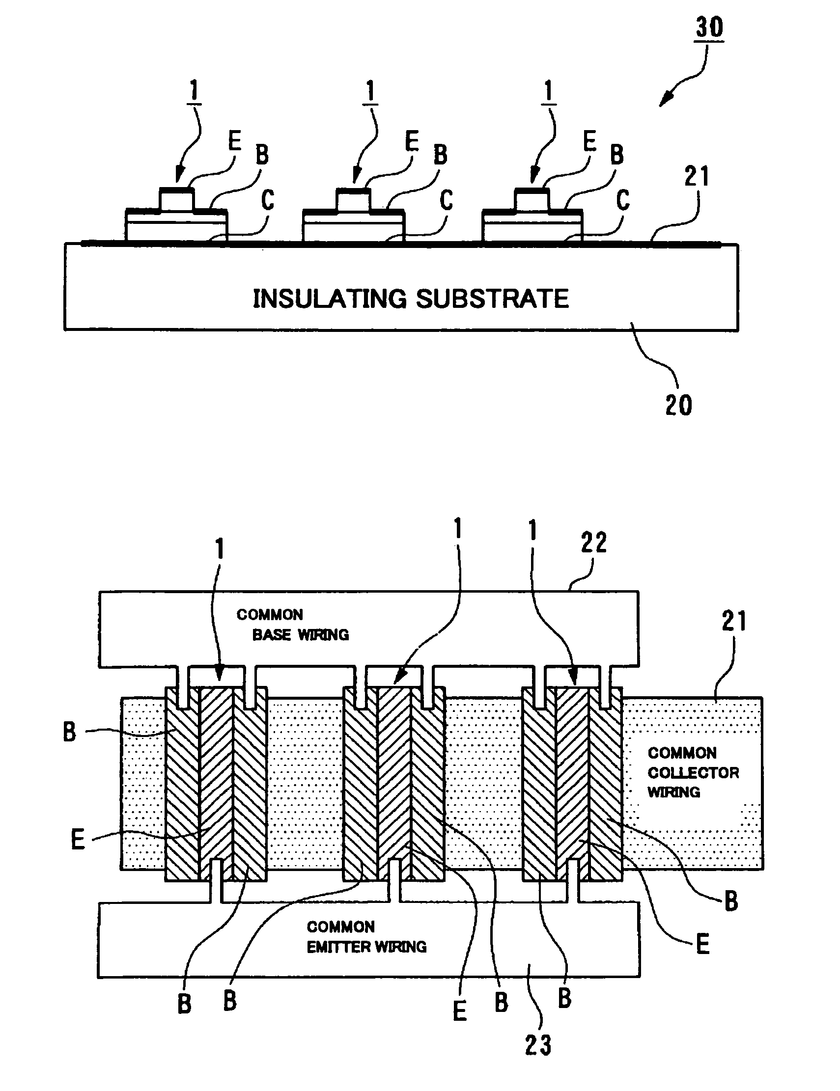
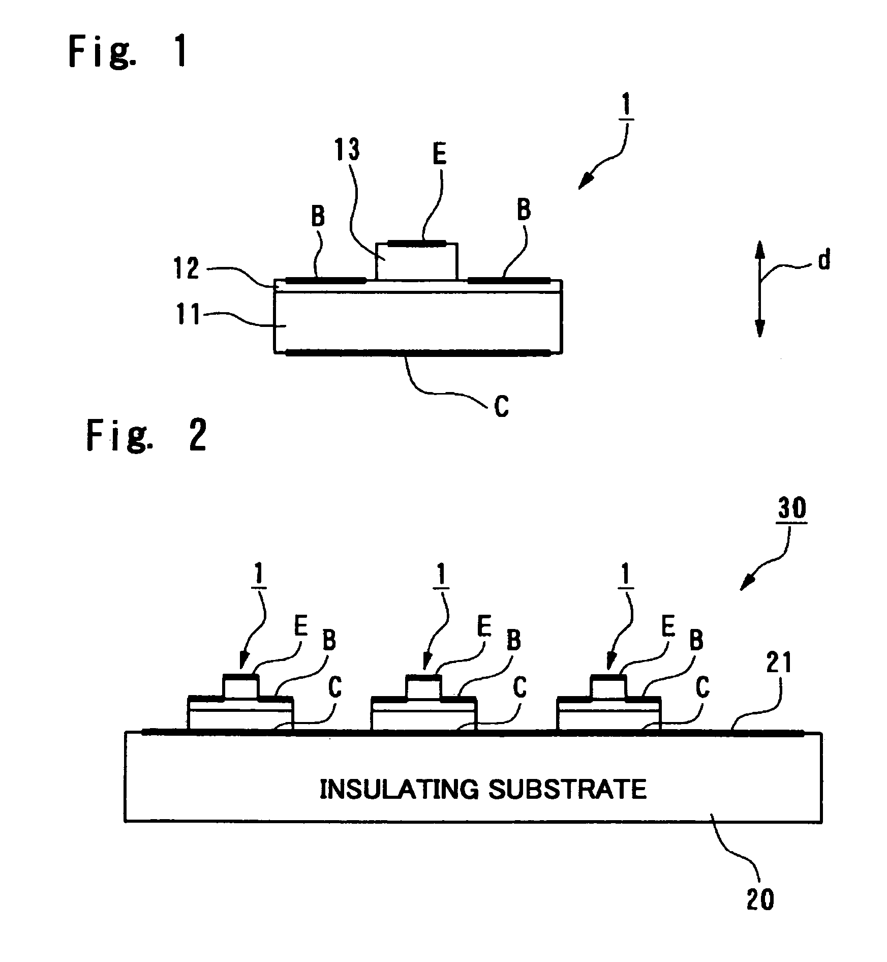
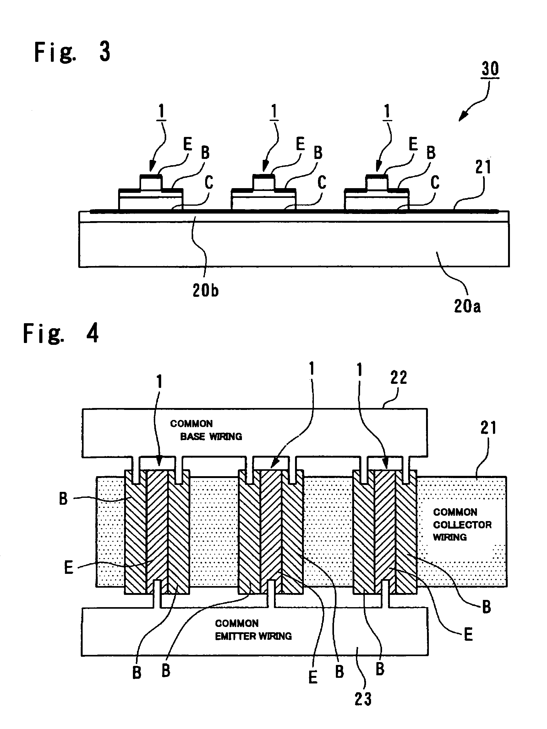
[0061]A hetero-bipolar transistor according to an embodiment of the present invention will now be described below with reference to the drawings.
[0062]FIG. 1 is a schematic side view showing one hetero-bipolar transistor element (unit element) according to the embodiment of the present invention. A unit element 1 includes a first layer 11 made of an N-type semiconductor, a second layer 12, which is provided on the first layer 11 and which is made of a P-type semiconductor, and a third layer 13, which is provided on the second layer 12 and which is made of an N-type semiconductor.
[0063]The second layer 12 can be formed on the entire top surface of the first layer 11, and is thinner than the first layer 11 and the third layer 13. The third layer 13 is provided in such a manner as to cross the center of the top surface of the second layer, and the area of the top surface is smaller than the area of the top surface of the first layer 11 and the second layer 12. The side surfaces of the ...
PUM
 Abstract
Description
Claims
Application Information