Characterizing circuit performance by separating device and interconnect impact on signal delay

a technology of interconnection and signal delay, applied in the field of integrated circuit testing, can solve the problems of inability to detect problems, time-consuming technique, and low ideal “external” measurement technique, and achieve the effect of efficient identification of problematic components

Active Publication Date: 2006-09-19
XILINX INC
View PDF24 Cites 16 Cited by
  • Summary
  • Abstract
  • Description
  • Claims
  • Application Information

AI Technical Summary

Benefits of technology

[0012]By embedding component-specific test circuitry within an IC, the invention enables efficient identification of problematic components within the IC. According to an embodiment of the invention, an IC includes multiple embedded test circuits, with each embedded test circuit including a ring oscillator coupled to a test load. The test load is either a direct short in the ring oscillator chain, or else is an interconnect structure that simulates one of the interconnect layers within the IC, such as a metal meander line or a contact / via chain.
[0014]According to an embodiment of the invention, the IC can be a programmable device, such as a field programmable gate array (FPGA), in which case the IC itself can be configured to collect the actual measurements of output delays from the embedded test circuits. By performing this type of “on-chip” measurement, the interface, speed, and accuracy limitations associated with conventional external measurement systems can be avoided.

Problems solved by technology

Unfortunately, this “external” measurement technique can be less than ideal in many circumstances.
Also, because the frequency measurement must be taken by an external measurement system (via test pad 132), the technique can be very time consuming.
This makes it infeasible to test all the ICs on a wafer (conventional testing systems typically only inspect about five dies per wafer), and so localized manufacturing problems may not be detected.
These measurement inaccuracies can significantly skew the final measurement results.
However, perhaps the most significant limitation associated with this conventional measurement technique is that it only provides a “bulk” reading of IC performance, and there is no way to determine the actual source of any unexpected signal propagation delays.
This is problematic, since any subsequent troubleshooting of IC performance degradation must therefore involve a comprehensive, and hence inefficient, methodology that examines all the different IC components.

Method used


Image

  • Characterizing circuit performance by separating device and interconnect impact on signal delay
  • Characterizing circuit performance by separating device and interconnect impact on signal delay
  • Characterizing circuit performance by separating device and interconnect impact on signal delay

Examples


Embodiment Construction

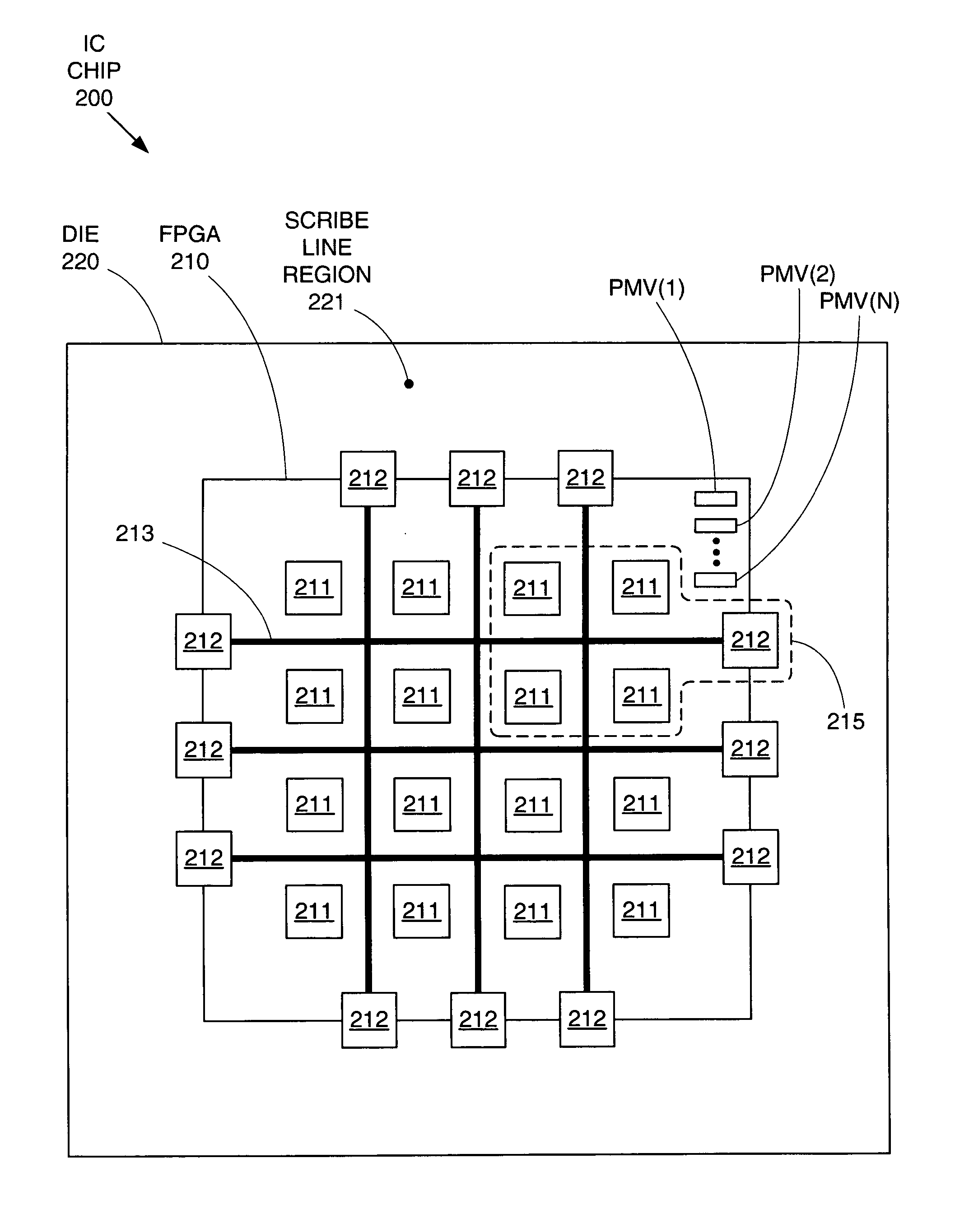
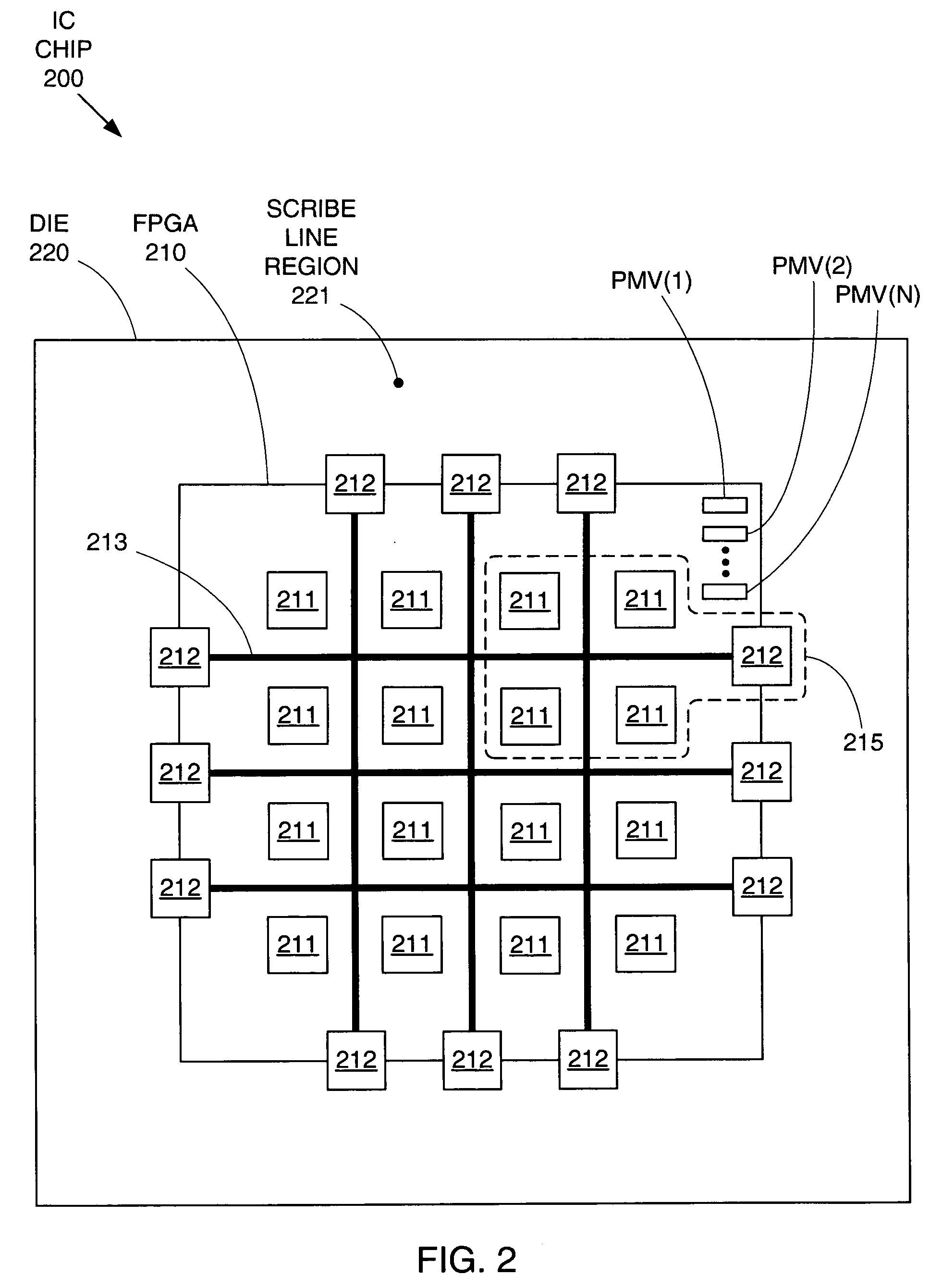
[0025]By creating a set of embedded test structures within an IC, the invention allows the performance of the IC to be determined by solving a simple set of linear equations. By analyzing the measurements from the different embedded test structures, the source(s) of any performance degradation can be isolated and identified. Furthermore, by embedding the test structures within the IC (rather than forming them in the scribe line region of the die), the measurement problems associated with external measurement systems (described above) can be avoided.

[0026]FIG. 2 shows a diagram of an IC chip 200 that includes an FPGA 210 formed on a die 220. Note that while IC chip 200 includes an FPGA for exemplary purposes, the invention can be used with any type of integrated circuit. For example, FPGA 210 could be replaced with a CPLD or other type of programmable logic IC. Note further that while some benefits of the invention (such as on-board measurement, described in greater detail below) are...


PUM


Abstract

An integrated circuit (IC) includes multiple embedded test circuits that all include a ring oscillator coupled to a test load. The test load either is a direct short in the ring oscillator or else is a interconnect load that is representative of one of the interconnect layers in the IC. A model equation is defined for each embedded test circuit, with each model equation specifying the output delay of its associated embedded test circuit as a function of Front End OF the Line (FEOL) and Back End Of the Line (BEOL) parameters. The model equations are then solved for the various FEOL and BEOL parameters as functions of the test circuit output delays. Finally, measured output delay values are substituted in to these parameter equations to generate actual values for the various FEOL and BEOL parameters, thereby allowing any areas of concern to be quickly and accurately identified.

Description

BACKGROUND OF THE INVENTION[0001]1. Field of the Invention[0002]The invention relates to the field of integrated circuit testing, and in particular to a system and method for determining the signal delay contributions from specific process layers.[0003]2. Related Art[0004]The performance of an integrated circuit (IC) is largely determined by its timing characteristics (i.e., the speed at which signals propagate through the IC). This signal propagation speed is typically analyzed via standalone testing systems that interface with dedicated test structures formed on the IC chip. Note that the term “IC chip” refers to the combination of the IC (i.e., the circuit structures and devices that provide the desired functionality, such as a field programmable gate array (FPGA) or an complex programmable logic device (CPLD)) and the die, or substrate, on which the IC is formed. Because a large number of IC chips are manufactured simultaneously on a single wafer, the die area is larger than the...

Claims


Application Information

Patent Timeline
Patent Type & Authority Patents(United States)
IPC IPC(8): G01R31/28G01R31/3185G01R31/3187
CPCG01R31/2882G01R31/3187G01R31/318516G01R31/318511
Inventor YUAN, XIAO-JIEHART, MICHAEL J.LING, ZICHENG G.YOUNG, STEVEN P.
Owner XILINX INC
Why Eureka
Try Eureka