Liquid crystal display and method of manufacturing the same

a technology of liquid crystal display and liquid crystal, which is applied in the field of liquid crystal display, can solve the problems of delay in response speed and slow halftone response from black to dark gray, and achieve the effects of improving delay in response speed, low gray level, and increasing halftone response speed

Inactive Publication Date: 2006-09-19
SHARP KK
View PDF9 Cites 15 Cited by
  • Summary
  • Abstract
  • Description
  • Claims
  • Application Information

AI Technical Summary

Benefits of technology

[0010]The present invention is made in view of the aforementioned problem, and its object is to provide a liquid crystal display which makes it possible to increase the speed of halftone response by improving a delay in response speed at low gray levels and realizes very reliable image display with moving image performance capable of being used without a sense of incongruity as compared with that of a CRT.

Problems solved by technology

The LCD is excellent in contrast and color reproduction at the front, but still has a big problem as concerns a viewing angle and moving image performance (response characteristic).
However, its application to the TV or the AV PC is considered, there is a problem that halftone response from black to dark gray is slow.
This delay in response speed at low gray levels is a problem related to the basic construction of the MVA mode, and is a fateful disadvantage.

Method used


Image

  • Liquid crystal display and method of manufacturing the same
  • Liquid crystal display and method of manufacturing the same
  • Liquid crystal display and method of manufacturing the same

Examples


first embodiment

[0091](First Embodiment)

[0092]First, the first embodiment of the present invention will be explained.

[0093]In this embodiment, an MVA mode liquid crystal display is exemplified.

[0094]Schematic Construction of Liquid Crystal Display

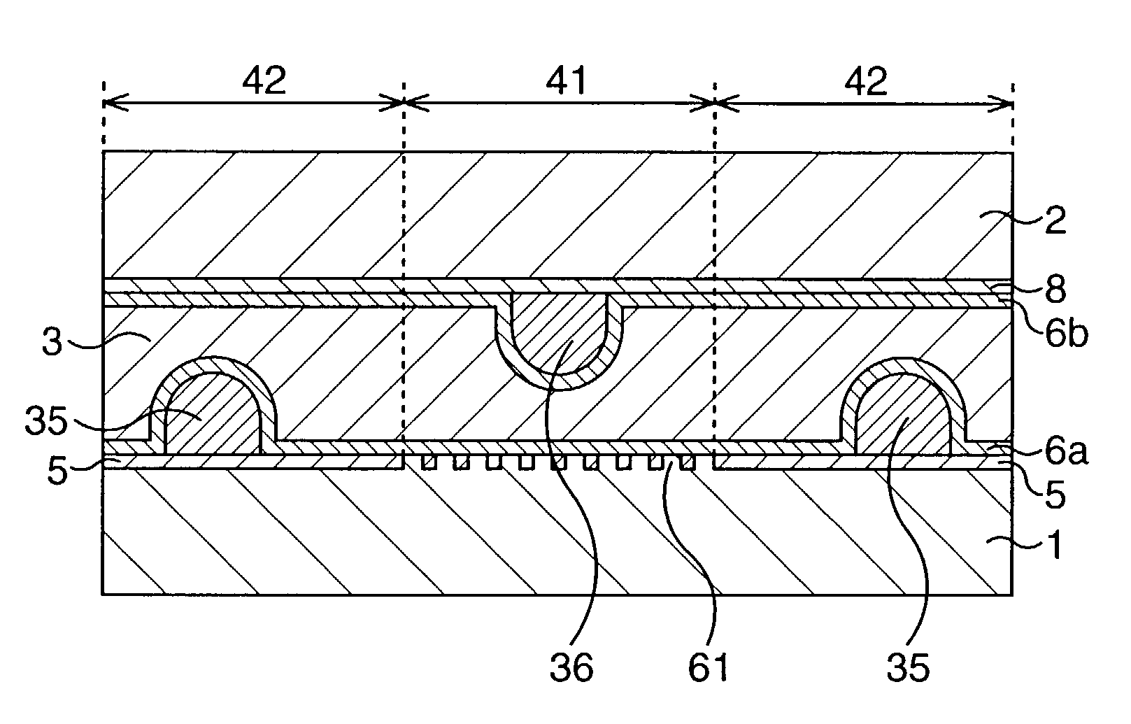
[0095]FIG. 1 is a sectional view showing the schematic main construction of a liquid crystal display of the present invention.

[0096]This liquid crystal display is constructed including a pair of transparent glass substrates 1 and 2 which face each other with a predetermined space therebetween, and a liquid crystal layer 3 sandwiched between the transparent glass substrates.

[0097]A plurality of ITO pixel electrodes 5 are formed on one transparent glass substrate 1 with an insulating layer 4 therebetween, and a transparent liquid crystal alignment film 6a is formed so as to cover the ITO pixel electrodes 5. A color filter 7, an ITO common electrode 8, and a liquid crystal alignment film 6b are stacked in sequence on the other transparent glass substrate 2. T...

experiment 1

[0110

[0111]FIGS. 4A and 4B are schematic views showing the main construction of a liquid crystal display of the experiment 1. Here, FIG. 4A is a plan view, and FIG. 4B is a sectional view.

[0112]In this experiment, as shown, on the pixel electrode 5 above the transparent glass substrate 1, slit-shaped fine electrode patterns 21, which are patter-formed in the shape of the fine teeth of a comb bilaterally symmetrical with respect to band-shaped portions, are formed at even intervals. Moreover, band-shaped dielectric layers 22 are pattern-formed at even intervals in the display pixel so as to cover the fine electrode patterns 21 on the pixel electrode 5. Although not shown, the alignment film 6a is formed to cover these dielectric layers 22. By the existence of the dielectric layer 22 and the fine electrode pattern 21 complementing this, a portion formed with these layer and fine electrode is a high threshold voltage region 23, and relatively, a low threshold voltage region 24 where th...

experiment 2

[0118

[0119]FIGS. 8A and 8B are schematic views showing the main construction of a liquid crystal display of the experiment 2, FIG. 8A is a plan view, and FIG. 8B is a sectional view.

[0120]In the experiment 1, a case where the dielectric layers 22 are provided on the pixel electrode 5 formed with the fine electrode patterns 21, above the transparent glass substrate 1 is shown. In this experiment, however, to simplify the process, the formation of the fine electrode patterns 21 are omitted, the dielectric layers 22 are provided on the pixel electrode 5 formed with only band-shaped slits 25 having a width of about 10 μm, and similarly to the experiment 1, the effect of partial response and the dependence on dielectric layer thickness are investigated.

[0121]FIGS. 9A and 9B are microphotographs showing the alignment state of liquid crystals in the construction of the experiment 2.

[0122]As shown, partial response is recognized when alignment in the application of a voltage of 3.0 V is obs...


PUM

PropertyMeasurementUnit
thicknessaaaaaaaaaa
voltageaaaaaaaaaa
widthaaaaaaaaaa

Abstract

A liquid crystal display including a pair of substrates having electrodes and a liquid crystal layer sandwiched between the substrates. A bank-shaped projection made of an insulating material is formed on the electrode, and each of the display pixels is divided into two or more regions having different capacitances by capacitive coupling. Additionally, voltages corresponding to the capacitances are applied to the respective regions in the application of a driving voltage.

Description

CROSS-REFERENCE TO RELATED APPLICATIONS[0001]This application is based upon and claims priority of Japanese Patent Application Nos. 2001-272355, filed on Sep. 7, 2001 and 2001-398317, filed on Dec. 27, 2001, the contents being incorporated herein by reference.BACKGROUND OF THE INVENTION[0002]1. Field of the Invention[0003]The present invention relates to a liquid crystal display constructed by sandwiching a liquid crystal layer between a pair of substrates having electrodes and a method of manufacturing the same, and particularly relates to a liquid crystal display which uses liquid crystals having negative dielectric constant anisotropy.[0004]2. Description of the Related Art[0005]A liquid crystal display (LCD) is currently utilized for the most purposes among flat panel displays. The display quality of the LCD, whose application to a large screen TV or a product such as called an AV personal computer into which a PC and a TV are integrated as well as a personal computer (PC), a wo...

Claims


Application Information

Patent Timeline
Patent Type & Authority Patents(United States)
IPC IPC(8): G02F1/133G02F1/1337G02F1/1333G02F1/1343G02F1/1368G02F1/139H01L21/28H01L21/336H01L29/786
CPCG02F1/133707G02F1/134309G02F2203/30G02F2001/133757G02F1/1393G02F1/133757G02F1/1337
Inventor TAKEDA, ARIHIRONAKAMURA, KIMIAKI
Owner SHARP KK
Why Eureka
Try Eureka