Post-layout optimization in integrated circuit design

a technology of integrated circuits and layouts, applied in computer aided design, program control, instruments, etc., can solve problems such as inability to adjust incrementally, long delays, and signal degradation, and achieve unacceptable delays and signal degradation

Active Publication Date: 2006-09-19
XILINX INC
View PDF5 Cites 45 Cited by
  • Summary
  • Abstract
  • Description
  • Claims
  • Application Information

AI Technical Summary

Problems solved by technology

Additionally, placing connected components close to one another generally improves the performance of the circuit, since long interconnect paths are associated with excess capacitance and resistance, resulting in longer delays.
On the other hand, if verification is not successful, then incremental modifications to the design may be necessary, after which the design must again pass through some or all of the CAD flow.
If their solutions are not optimal, there may be excessive capacitance and resistance, leading to unacceptable delays and signal degradation.

Method used


Image

  • Post-layout optimization in integrated circuit design
  • Post-layout optimization in integrated circuit design
  • Post-layout optimization in integrated circuit design

Examples


Embodiment Construction

[0015]The present invention relates to a new method for post-layout timing optimization. In the following description, numerous specific details are set forth in order to provide a more thorough understanding of the present invention. However, it will be apparent to one skilled in the art that the present invention may be practiced without these specific details. In other instances, well-known features have not been described in detail in order to avoid obscuring the present invention.

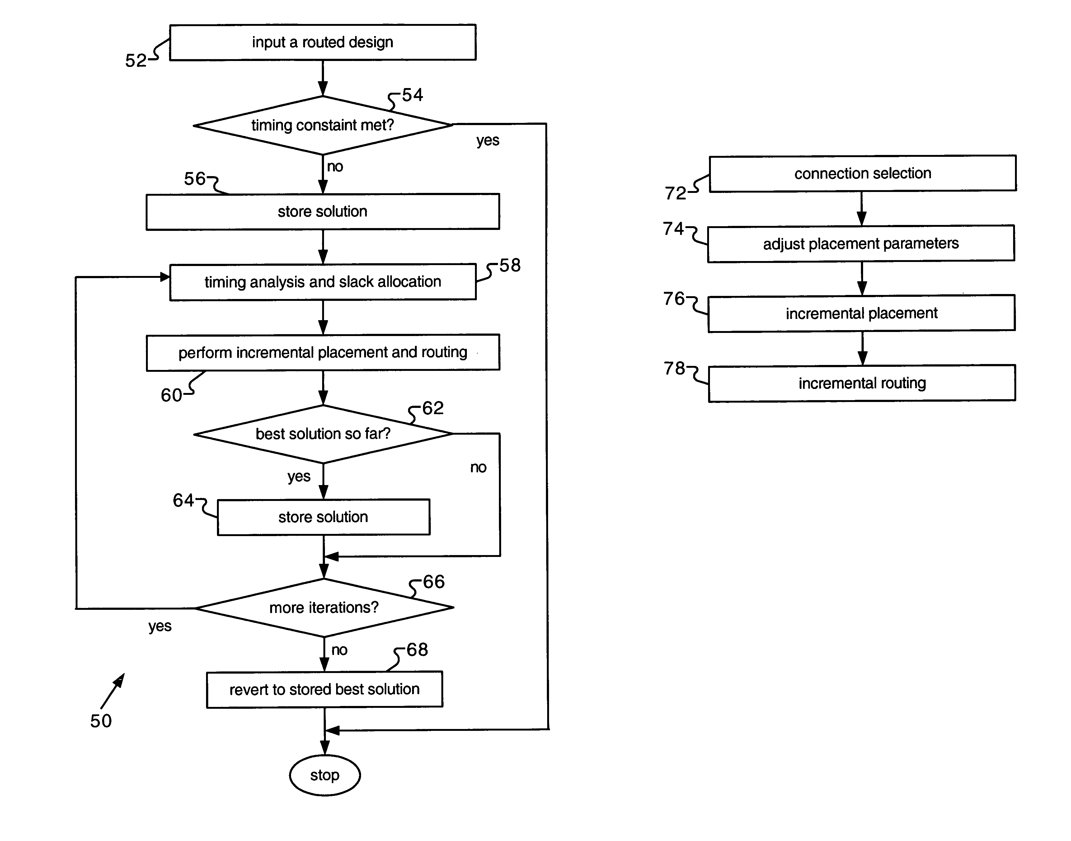
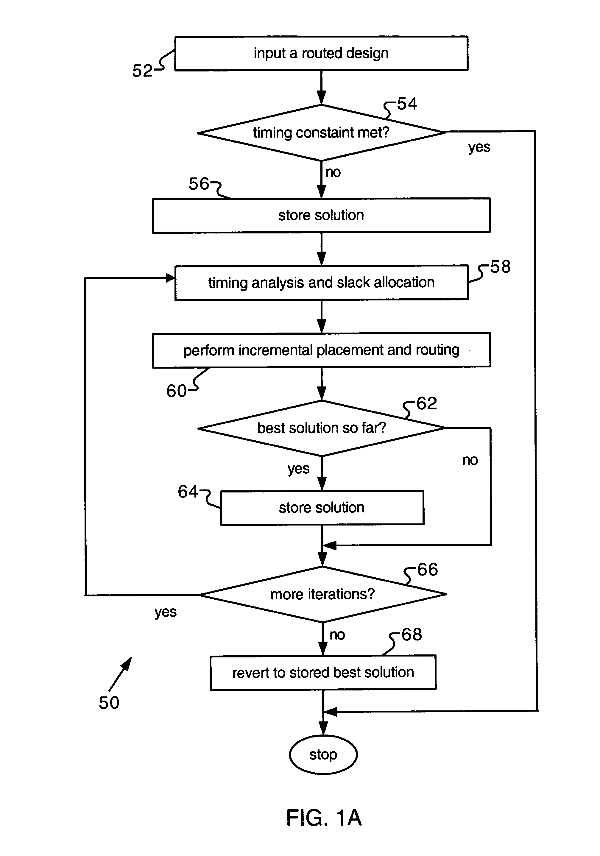
[0016]FIG. 1A is a flow chart showing an overview of a post-layout timing optimization operation 50 of the present invention. In step 52, a routed design is accepted for processing. In step 54, timing analysis is performed to determine whether timing constraints have been met. If the constraints have been met, operation 50 terminates. If the constraints have not been met, the original placement and routing solution for the design is stored (step 56). In step 58, timing analysis and slack allocation ope...


PUM


Abstract

A method for post-layout timing optimization is disclosed. The method performs timing analysis on a design to obtain timing information such as critical paths and slack values. Incremental placement based on the timing information is performed. A new routed design is generated by applying incremental routing to the result of incremental placement. The routed design is stored if its performance is better than the previous routed design. The above steps are repeated until a predetermined criterion is met.

Description

FIELD OF THE INVENTION[0001]This invention relates to computer-aided design (CAD), and specifically, to a method for post-layout optimization of the placement and routing of an integrated circuit.BACKGROUND OF THE INVENTION[0002]The design process for integrated circuits contains a number of well known sequential operations. Initially, the proposed functionality of a circuit is analyzed by one or more chip designers. These designers then use design capture tools to describe the logical components of the circuit and their interactions. This step involves generating a description of the design to be implemented in an appropriate machine-readable form. One of the commonly used methods for specifying a design is a hardware description language (HDL). This language contains specific functions and syntax to allow complex hardware structures to be described in a compact and efficient way. Computer-aided design tools are available to compile or synthesize the HDL description specifying the ...

Claims


Application Information

Patent Timeline
Patent Type & Authority Patents(United States)
IPC IPC(8): G06F17/50
CPCG06F17/5077G06F17/5072G06F30/392G06F30/394G06F30/3312G06F2119/12
Inventor ANDERSON, JASON H.KALMAN, SANDOR S.VERMA, VINAY
Owner XILINX INC
Why Eureka
Try Eureka