Stacked capacitor having parallel interdigitized structure for use in thin film transistor liquid crystal display

Active Publication Date: 2006-09-26
AU OPTRONICS CORP
View PDF5 Cites 190 Cited by
  • Summary
  • Abstract
  • Description
  • Claims
  • Application Information

AI Technical Summary

Benefits of technology

[0013]It is an advantage that the present invention capacitor structure replaces the conventional planer capacitor of two-layered electrode plates with three stacked capacitors of four prior art conductive layers in conjunction as four-layered electrode plates. Since these three capacitors are connected in parallel with one another, the capacitance value of the equivalent capacitor is equal to the sum of the capacitance values of these three capacitors. The area of the present invention capacitor structure is thus only approximately one third of the area of the prior art capacitor structure used to store the same number of ch

Problems solved by technology

Under the limitation of insufficient aperture ratio in the pixel, special processing or consideration is

Method used


Image

  • Stacked capacitor having parallel interdigitized structure for use in thin film transistor liquid crystal display
  • Stacked capacitor having parallel interdigitized structure for use in thin film transistor liquid crystal display
  • Stacked capacitor having parallel interdigitized structure for use in thin film transistor liquid crystal display

Examples


Embodiment Construction

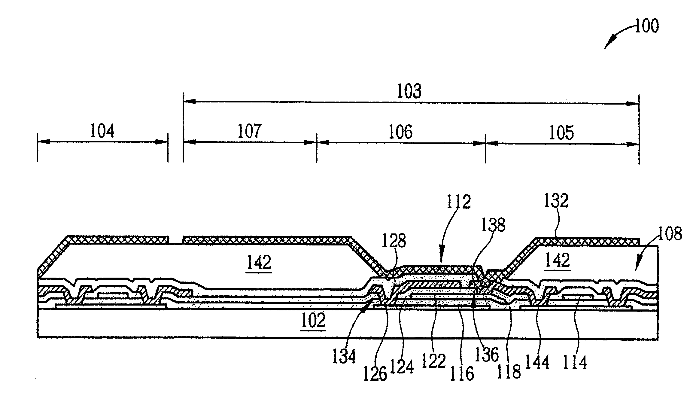
[0019]Referring to FIG. 3, FIG. 3 is a structural schematic diagram of a thin film transistor liquid crystal display 100 according to the present invention. As shown in FIG. 3, the present invention thin film transistor liquid crystal display 100 comprises a substrate 102. The substrate 102, composed of transparent materials, is an insulating substrate, and the substrate 102 comprises a glass substrate, a quartz substrate, or a plastic substrate. A pixel array area 103 and a periphery circuit area 104 are included on a surface of the substrate 102. A thin film transistor area 105, a capacitor area 106, and an aperture region 107 are included in the pixel array area 103. The thin film transistor area 105 is used for disposing a thin film transistor 108, and the capacitor area 106 is used for disposing a storage capacitor 112. Since a gate 114 of the thin film transistor 108 is composed of a low temperature polysilicon material, the thin film transistor 108 is a low temperature polysi...


PUM


Abstract

A capacitor structure includes a first conductive layer, a first insulating layer disposed on a substrate in sequence, a second conductive layer disposed on portions of the first insulating layer, a second insulating layer disposed on the second conductive layer and the first insulating layer, a third conductive layer disposed on portions of the second insulating layer, a third insulating layer disposed on the third conductive layer and the second insulating layer, and a fourth conductive layer disposed on the third insulating layer. The third conductive layer and the fourth conductive layer are electrically connected to the first conductive layer and the second conductive layer through at least one first contact hole adjacent to the second conductive layer and at least one second contact hole, respectively.

Description

BACKGROUND OF INVENTION[0001]1. Field of the Invention[0002]The present invention relates to a capacitor structure, and more particularly, to a capacitor structure applied to a thin film transistor liquid crystal display (TFT-LCD) to improve contrast of the display by increasing capacitance value and aperture ratio.[0003]2. Description of the Prior Art[0004]Currently, liquid crystal displays(LCDs)area mature flat panel display technology. Applications for liquid crystal displays are extensive and include mobile phones, digital cameras, video cameras, notebooks, and monitors. Due to high quality display requirements and the expansion of new application fields, the LCD has developed toward high quality, high resolution, high brightness, and low price. A low temperature polysilicon thin film transistor liquid crystal display (LTPS-TFTLCD) is one type of thin film transistor liquid crystal display. The low temperature polysilicon thin film transistor liquid crystal display, being active...

Claims


Application Information

Patent Timeline
IPC IPC(8): G02F1/136G02F1/1362H01L27/12
CPCH01L27/12G02F1/136213
Inventor CHANG, CHIH-CHINYEH, KUANG-CHAO
Owner AU OPTRONICS CORP
Why Eureka
Try Eureka