Capacitance multiplier

a technology of capacitance multiplier and multiplier, which is applied in the direction of process and machine control, computation using denominational number representation, instruments, etc., can solve the problem that the capacitance multiplier of fig. 1a may not operate with stability, and achieve the effect of reducing noise and more stable generation of multiplied capacitan

Active Publication Date: 2006-09-26
SAMSUNG ELECTRONICS CO LTD
View PDF5 Cites 3 Cited by
  • Summary
  • Abstract
  • Description
  • Claims
  • Application Information

AI Technical Summary

Benefits of technology

[0014]Accordingly, a capacitance multiplier includes self-biasing, cascode loads, and / or a plurality of multiplying paths for efficiency in generating the multiplied capacitance with higher bandwidth, reduced area, and / or higher output resistance.
[0020]In this manner, with the active load being self-biasing, a separate current bias is not used for minimizing area of the capacitance multiplier. In addition, with use of cascodes, the output resistance is increased for higher charging / discharging efficiency.
[0022]In such an embodiment, a total capacitance at the first node is a sum of the respective second capacitances for the plurality of capacitors such that effects of noise may be reduced for more stable generation of the multiplied capacitance.

Problems solved by technology

As a result, when the PMOS and NMOS transistors MP2 and MN2 are mismatched, the capacitance multiplier of FIG. 1A may not operate with stability.
Unfortunately, the capacitance multiplier of FIGS. 1A and 1B has a relatively narrow bandwidth and requires a relatively high area for a bias circuit comprised of the current source for IBIAS and the extra MOS transistors MP3, MN3, and MN4.

Method used


Image

  • Capacitance multiplier
  • Capacitance multiplier
  • Capacitance multiplier

Examples


Embodiment Construction

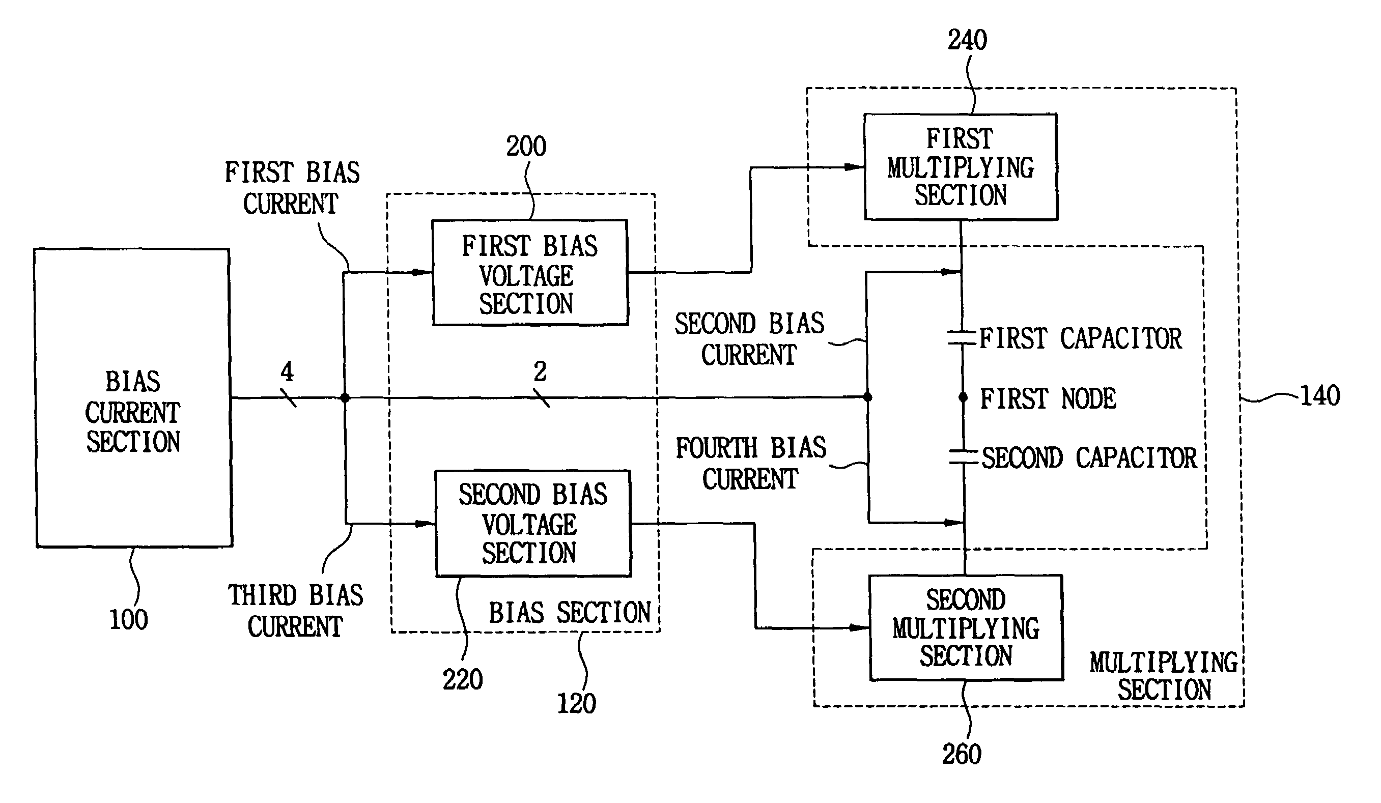
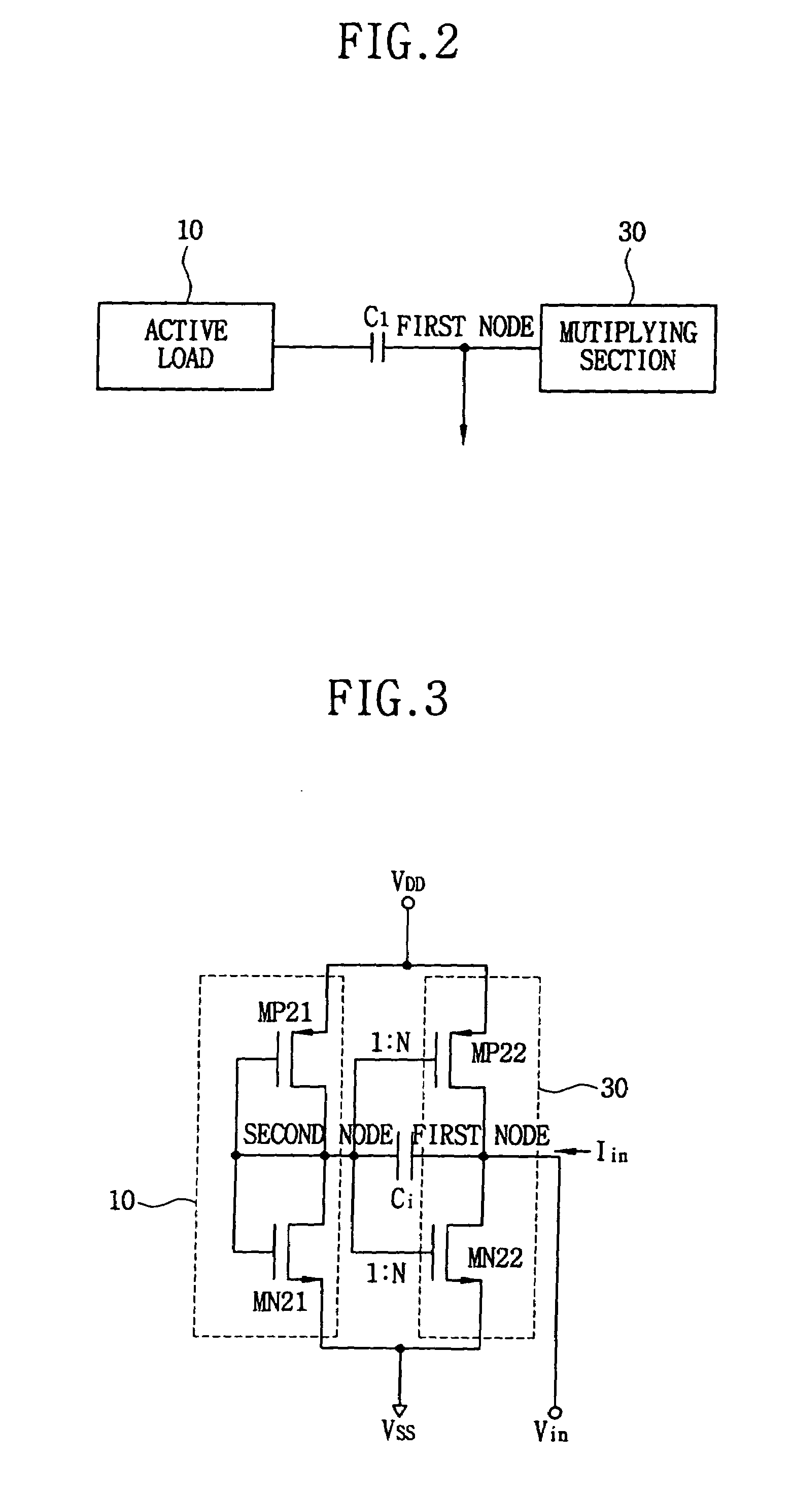
[0040]FIG. 2 is a block diagram of a capacitance multiplier with a self-biasing active load 10 according to an embodiment of the present invention. Referring to FIG. 2, the capacitance multiplier also includes a capacitor C, and a multiplying section 30. The active load 10 is self-biasing because the active load 10 generates a bias voltage without using a separate bias current, for a reduced area and higher stability. A first node is an I / O (input-output) terminal having the multiplied capacitance generated thereon. The multiplying section 30 multiplies a capacitance, C, of the capacitor C1.

[0041]FIG. 3 is a circuit diagram for an example implementation of the capacitance multiplier of FIG. 2. Referring to FIG. 3, the active load 10 includes a first PMOS transistor MP21 and a first NMOS transistor MN21. The first PMOS transistor MP21 has a source coupled to a high voltage source VDD, and has a gate and a drain coupled together to a second node. The first NMOS transistor MN21 has a s...


PUM


Abstract

A capacitance multiplier includes a self-biasing active load for generating a stable bias voltage without a separate current bias. In addition, the capacitance multiplier includes a cascode load within a multiplying section for increasing the output resistance and in turn the charging / discharging efficiency. Furthermore, the capacitance multiplier is implemented with a plurality of multiplying paths to reduce effects of noise for more stable generation of the multiplied capacitance.

Description

BACKGROUND OF THE INVENTION[0001]This application claims priority under 35 USC § 119 to Korean Patent Application No. 2003-0063579 and Korean Patent Application No. 2004-0000228, filed on Sep. 15, 2003 and Jan. 5, 2004 respectively, the contents of which are incorporated herein in their entirety by reference.[0002]1. Field of the Invention[0003]The present invention relates generally to a capacitance multiplier, and more particularly to a capacitance multiplier having self-biasing, cascode loads, and / or a plurality of multiplying paths, for higher efficiency in generating the multiplied capacitance.[0004]2. Description of the Related Art[0005]A capacitance multiplier is a circuit that multiplies a capacitance of a capacitor. FIG. 1A is a circuit diagram illustrating a conventional capacitance multiplier, and FIG. 1B illustrates a small-signal model of the capacitance multiplier of FIG. 1A.[0006]Such a capacitance multiplier is discussed in detail in a document, Sergio Solis-Bustos, ...

Claims


Application Information

Patent Timeline
Patent Type & Authority Patents(United States)
IPC IPC(8): G05F1/10H03H11/48
CPCH03H11/483H03H11/48
Inventor KIM, YOUNG-JINHWANG, IN-CHULLEE, HAN-ILLEE, JAE-HEON
Owner SAMSUNG ELECTRONICS CO LTD
Why Eureka
Try Eureka