Method for wet etching of high k thin film at low temperature

a technology of high k thin film and low temperature, which is applied in the direction of semiconductor devices, electrical equipment, capacitors, etc., can solve the problems of leakage current, difficult to be etched, and difficult control of the fabrication process, so as to reduce the defect size, reduce the leakage current and the topology, and reduce the defect size

Inactive Publication Date: 2006-10-03
GRAND PLASTIC TECH +1
View PDF4 Cites 15 Cited by
  • Summary
  • Abstract
  • Description
  • Claims
  • Application Information

AI Technical Summary

Benefits of technology

[0009]Another object of the present invention is to provide a method of wet etching a high k film which has high selectivity with respect to silicon dioxide (SiO2), un-doped silicon glass (USG) and bulk silicon to reduced defects on USG in the isolation region, poly-Si gate and silicon of source / drain region, so that the leakage current and topology can be reduced.
[0010]The third object of the present invention is to provide a wet etch method at low temperature, which has acceptable etch rate, and the processing time can be reduced to increase throughput. In order to achieve the above objects, according to the first aspect of the present invention, a method using hydrofluoric acid (HF) and perchloric acid (HClO4) (or perbromic acid HBrO4, periodic acid HIO4) mixture for etching the high k film on silicon dioxide (SiO2) or poly-Si, the volume ratio is between 1:50 to 1:5000, the better is 1:1000 to 1:2500, at low temperature (0° C. to 100° C.), the etch rate of high k film is more than 10A / min. However the etch rate of SiO2, USG and poly-Si is below 10A / min, the selectivity is good enough.
[0011]According to the second aspect of the present invention is to provide a method for manufacturing CMOS logic devices with high k gate dielectric film. After the gate, the lightly doped source / drain and the side-well of the gate has been formed, using HF and HClO4 (or HBrO4, HIO4) mixture to etch the high k gate dielectric on the source / drain, would not hurt the USG in the shallow trench isolation region, the silicon surface of the source / drain region, the poly-Si gate and the metal gate or refractory metal silicide of the gate.
[0012]According to the third aspect of the present invention, is to provide a method for manufacturing DRAM with high k capacitor. After completed forming the transistor and lower electrode of a DRAM, and have deposited high k film as capacitor dielectric on the lower electrode, protect the bottom electrode and the high k film with photo resist, then remove the high k film by wet etch using HF and perchloric acid (HClO4) (or perbromic acid HBrO4, periodic acid HIO4) mixture at low temperature (0° C. to 100° C.), very good etch pattern can be obtained, the etching process will not form defect on the BPSG or PSG under the high k film. The etch rate of high k film is above 10A / min, but the etch rate of BPSG or PSG is under 10A / min.
[0013]According to the fourth aspect of the present invention, is to provide a method for manufacturing high k capacitors. After a blanket deposition of high k dielectric film on the substrate having a lower electrode, protect the lower electrode and high k film on the lower electrode with photo-resist, then remove the high k film by wet etch using HF and perchloric acid (or perbromic acid HBrO4, periodic acid HIO4) mixture at low temperature (0° C. to 100° C.). This etching process will not damage the silicon substrate or the isolation silicon dioxide.

Problems solved by technology

The fabrication process is more difficult to control.
Although they have an idea dielectric constant of 15-25, and more stable that they do not diffuse into the silicon active area, and the leakage current is less, but it is not easy to be etched.
Poor selectivity of dry etching causes leakage current, which due to defects on the surface of the source / drain.
The un-doped silicon glass (USG) and the silicon above the source / drain may form defects 14 since the selectivity is not high enough.
After the process is completed the leakage current of the device will increase.

Method used


Image

  • Method for wet etching of high k thin film at low temperature
  • Method for wet etching of high k thin film at low temperature
  • Method for wet etching of high k thin film at low temperature

Examples


first embodiment

[0033

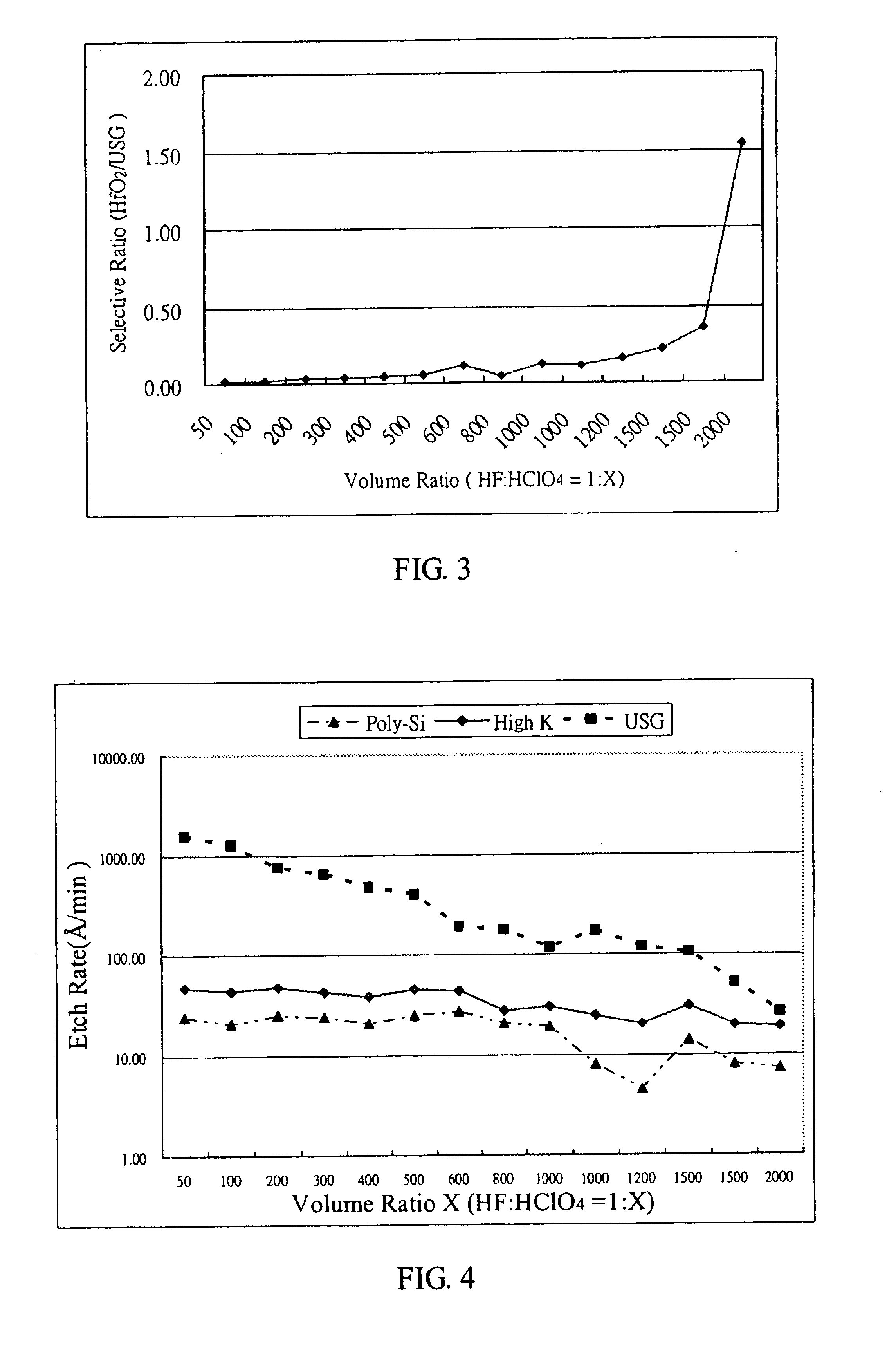
[0034]The etching of high k material (HfO2) film has been studied with different solution by the inventers. All the HfO2 film is deposited by Physical vapor deposition (PVD) or CVD, un-doped silicon glass (USG) or poly-Si is deposited by chemical vapor deposition (CVD), the thickness of the film before and after etching is measured by an n&k analyzer. Etching the high k film with H2SO4 at 160° C., the etch rate is 1.15˜5.25A / min and the selectivity to USG is 1:1, can be acceptable, but high temperature endurable wet bench is needed. Etching with pure phosphoric acid (H3PO4), pure perchloric acid (HClO4), pure hydrochloric acid (HCl), pure hydro bromide (HBr), pure hydroiodide (HI) or pure acitic acid (COOH)2, the etch rate is too low and can not be used. Etching with dilute hydrochloric (HF:H2O=1:2000), the etch rate of HfO2 is 1A / min, but the etch rate of USG is as high as 7A / min., the selectivity of 1:7 can not be acceptable, it will damage the USG in the shallow trench isola...

second embodiment

[0037

[0038]Refer to FIG. 5 to FIG. 15, which shows the process step of the manufacturing method of a CMOS 200. It is especially emphasis on the formation step and method of a high k gate. FIG. 5 shows the structure of a CMOS logic device 200. In the following description the silicon substrate is p-type, but n-type substrate or SOI (silicon on insulator) substrate can be used. The isolation of the second embodiment using shallow trench isolation is an example, but LOCOS isolation can be used. Tungsten silicide on poly-Si gate is used to reduce the gate resistance, but salicide like TiSi2 or CoSi2 can be used to replace WSiX. Also the gate is not limited to poly-Si gate, such as metal gate or refractory metal silicide can be used. The CMOS integration process which include the use of high k material should be included in the present invention.

[0039]In step of FIG. 6, the active area is defined by selectively formed the device isolation STI on the p-type silicon substrate, then forms t...

third embodiment

[0049

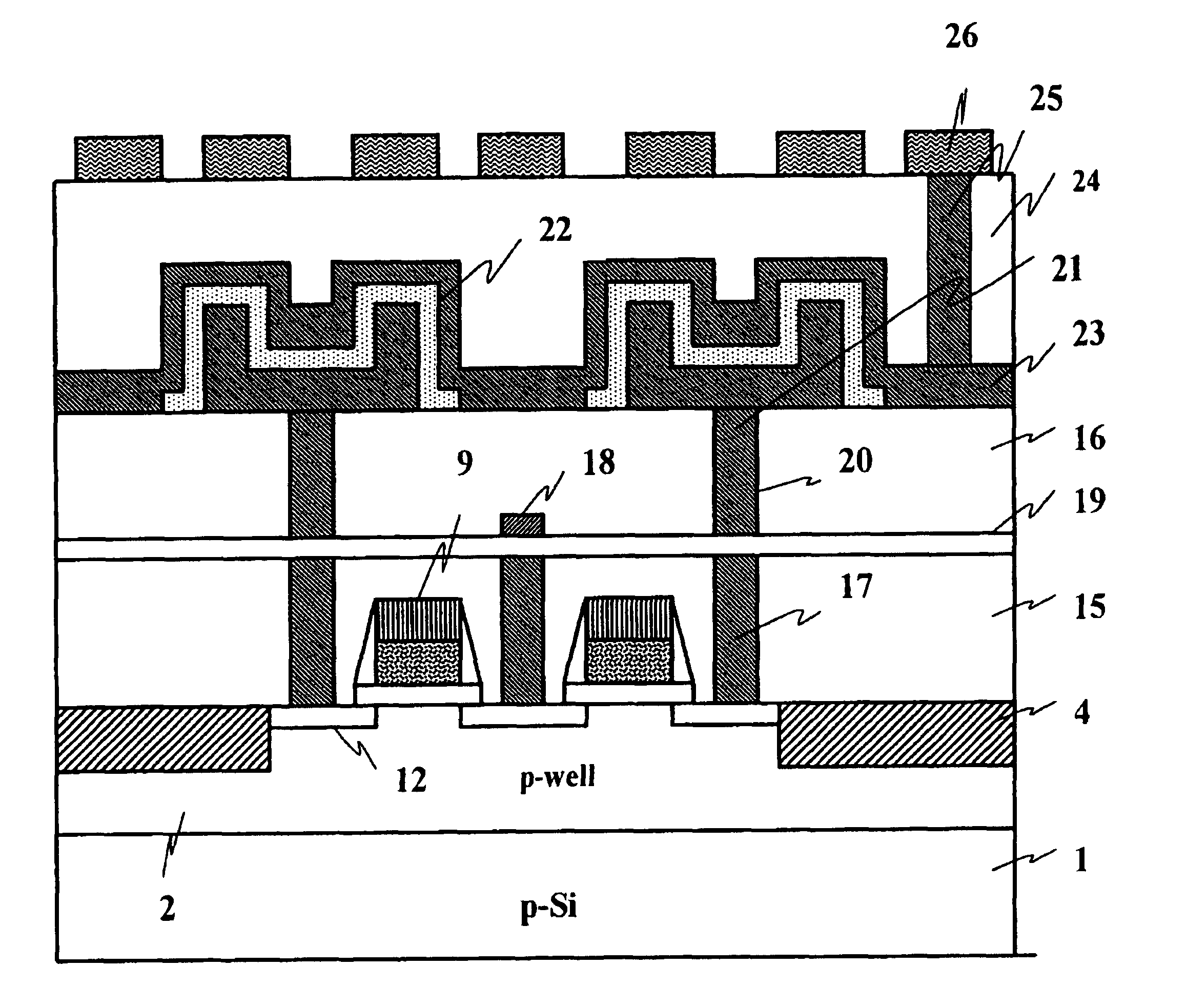
[0050]FIG. 16 is a cross section view of a DRAM having high k dielectric insulator (HfO2 or ZrO2) after forming a stack lower electrode of the capacitor and having deposited high k film (HfO2 or ZrO2) according to the present invention. After forming a shallow trench isolation 4 on the p-well 2, LDD source / drain (or n+ source / drain instead of LDD), gate 9, inter layer dielectric (ILD) 15, tungsten or poly-Si plug 17, BPSG inter metal dielectric (IMD) 16, silicon nitride etching stop layer 19 and lower electrode 21, then high k film 22 of the capacitor dielectric is deposited using PVD or CVD as shown in FIG. 16. The shape of the lower electrode is not limited to this stack type, other stack or trench capacitor can be used.

[0051]Then, as shown in FIG. 17, etch the high k film using HF and HClO4 (or HBrO4,, HIO4) as the etch solution and photo-resist PR5 as the protection mask to protect the lower electrode and the high k film on the electrode, in an etching tool by wet etching a...


PUM

PropertyMeasurementUnit
temperatureaaaaaaaaaa
dielectric constantaaaaaaaaaa
temperatureaaaaaaaaaa

Abstract

The present invention discloses an electrode structure of a light emitted diode and manufacturing method of the electrodes. After formed a pn junction of a light emitted diode on a substrate, a layer of SiO2 is deposited on the periphery of the die of the LED near the scribe line of the wafer, then a transparent conductive layer is deposited blanketly, then a layer of gold or AuGe etc. is formed with an opening on the center of the die. After forming alloy with the semiconductor by heat treatment to form ohmic contact, a strip of aluminum (Al) is formed on one side of the die on the front side for wire bonding and to be the positive electrode of the LED. The negative electrode is formed on the substrate by metal contact. Another form of the electrode structure of the present invention is making both the positive and negative electrodes on the front side of the LED by etching the p-type semiconductor of the pn junction and forming a strip of negative electrode on the n-type semiconductor, the positive electrode is formed on the p-type semiconductor.

Description

BACKGROUND OF THE INVENTION[0001]1. Field of the Invention[0002]The present invention relates to a semiconductor device manufacturing method and more particularly, to a method for wet etching of high k thin film at low temperature.[0003]2. Description of Relative Prior Art[0004]The recent development of semiconductor such as CMOS logic device or dynamic random access memory (DRAM), is preferable to increase the integration, increase the capacity, decrease the driving voltage etc., to meet the requirement of high speed, less delay. The design rule is more and more quickly reduced. It is a result that the thickness of the gate oxide is decreasing and approaching 60A or less. The fabrication process is more difficult to control. In a capacitor of a DRAM, a silicon dioxide insulator or an oxide-nitride-oxide (ONO) can not satisfy the need of the memory charge capacity, it is a trend that high dielectric film is used as the insulating film of a capacitor to replace the silicon dioxide or...

Claims


Application Information

Patent Timeline
Patent Type & Authority Patents(United States)
IPC IPC(8): H01L21/302H01L21/461H01L21/02H01L21/311H01L21/316H01L21/8242H01L27/108
CPCH01L21/31111H01L21/31641H01L21/31645H01L27/10814H01L27/10852H01L28/40H10B12/315H10B12/033H01L21/02189H01L21/02181
Inventor HO, HSIEH YUEWANG, CHIH-CHENGSHIH-YI, HSIAOTSUNG-KUEI, KANGTSUI, BING-YUEHUANG, CHIH-FENGLIANG, JANN-SHYANGTSAI, MING-HUANTAO, HUN-JANPERNG, BAW-CHING
Owner GRAND PLASTIC TECH
Why Eureka
Try Eureka