Semiconductor device having a strained raised source/drain

a technology of raised source and semiconductor, applied in the field of semiconductor devices, can solve the problems of poorly controlled recesses that are not suitable for large-scale manufacturing, the recesses of source/drain silicon must be controlled and reproducible, etc., and achieve the effect of tight tolerances in the recesses

Inactive Publication Date: 2006-10-03
GLOBALFOUNDRIES INC
View PDF21 Cites 14 Cited by
  • Summary
  • Abstract
  • Description
  • Claims
  • Application Information

AI Technical Summary

Benefits of technology

[0005]The present invention provides a technique that solves the aforementioned problem by presenting a manufacturable way to recess silicon that employs an end point detection method for the recess etch and allows tight tolerances on the recess. The present invention also provides a semiconductor structure that is fabricated by the aforementioned method.

Problems solved by technology

One problem with this approach is that the recess of the source / drain silicon must be controlled and reproducible to obtain a manufacturable process.
These methods suffer from the fact that the etch rate may vary from day to day and also the surface of the silicon being etched is variable and may have a variable induction time before etching begins.
This leads to a poorly controlled recess that is not suitable for largescale manufacturing.

Method used


Image

  • Semiconductor device having a strained raised source/drain
  • Semiconductor device having a strained raised source/drain
  • Semiconductor device having a strained raised source/drain

Examples


Embodiment Construction

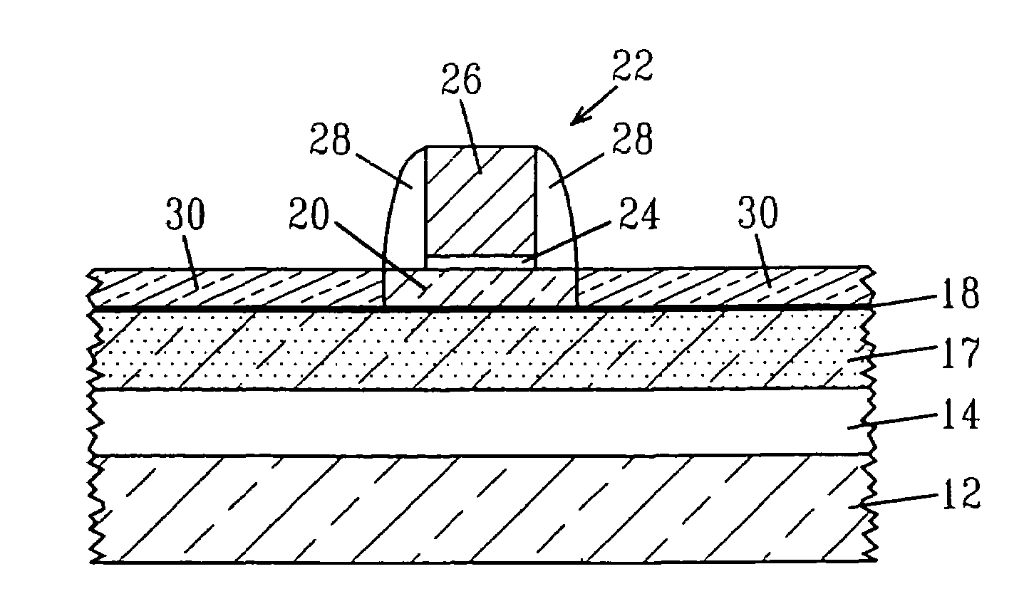
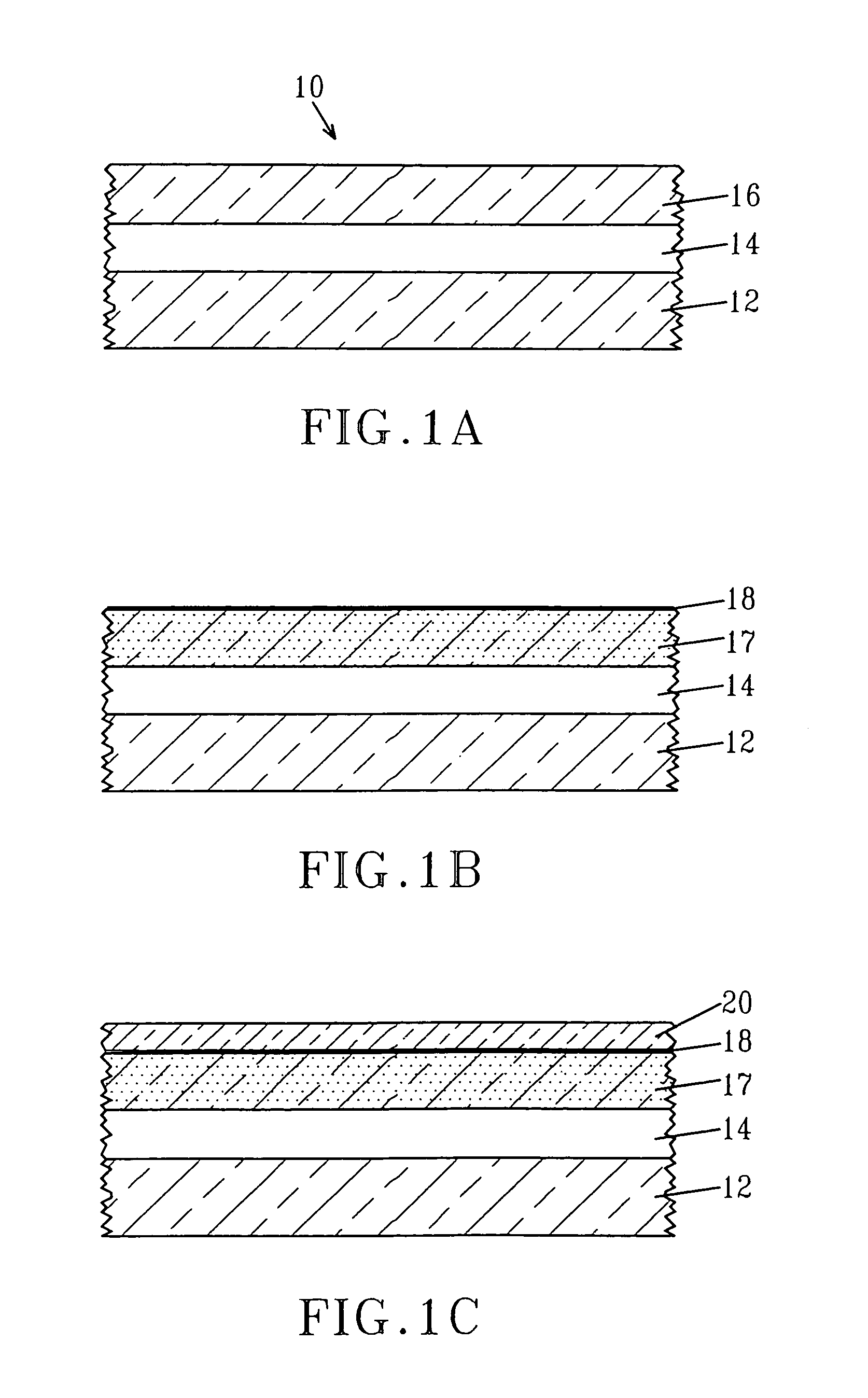
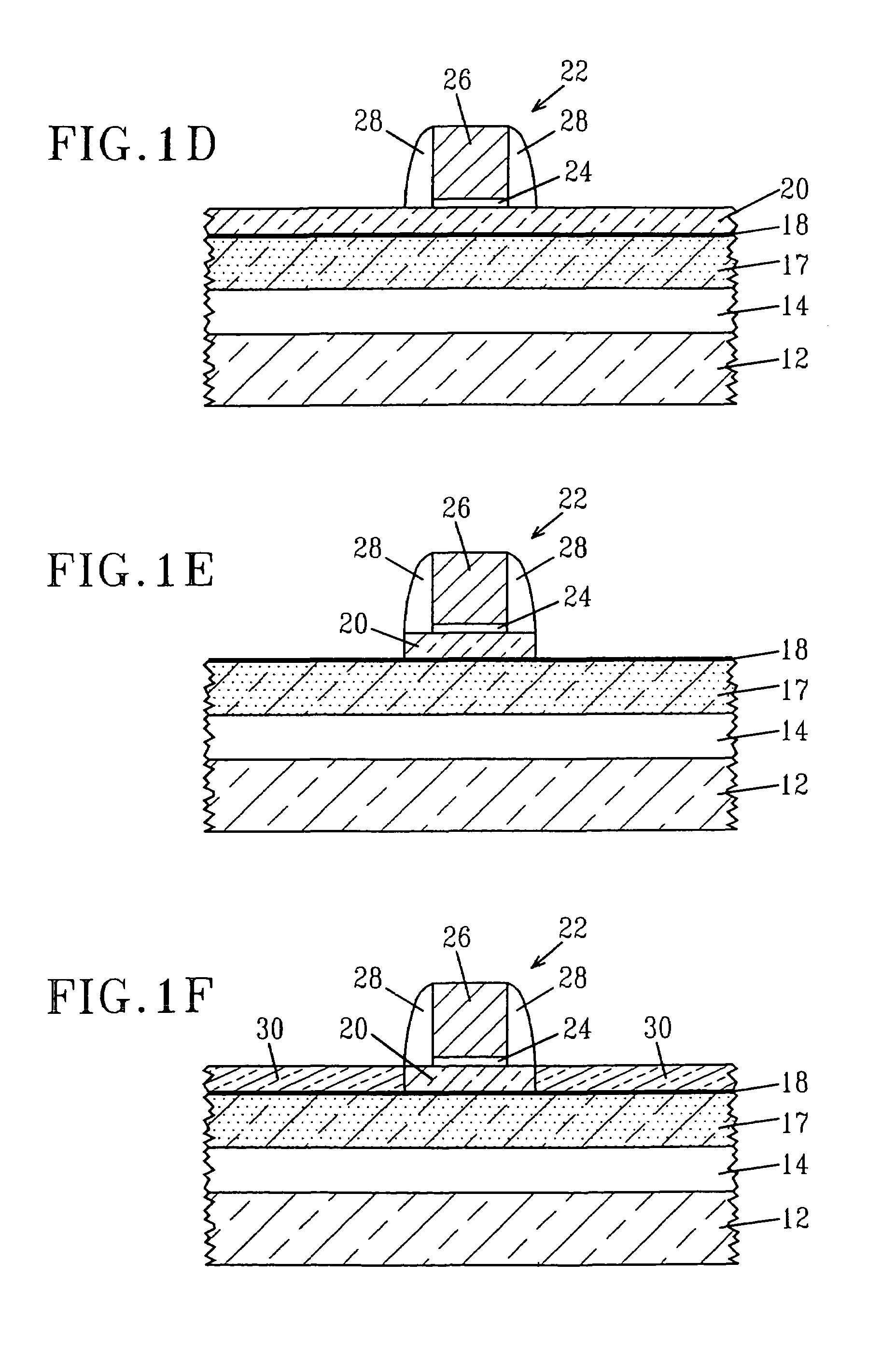
[0010]The present invention, which provides a manufacturable recessed raised strained source / drain structure and a process for fabricating the same, will now be described in greater detail by referring to the drawings that accompany the present application.

[0011]Although the description and drawings illustrate the use of an SOI substrate as the initial substrate, other semiconductor substrates besides SOI can be used. Illustrative examples of other initial substrates that can be used in the present invention include, but are not limited to: Si, SiC, SiGe, SiGeC, Ge, InAs, InP as well as other III / V or II / VI compound semiconductors. The initial substrate may also comprise a SiGe-on-insulator substrate or any other layered semiconductor, such as, for example, Si / SiGe.

[0012]Although other semiconductor substrates can be employed, it is preferred to use an SOI substrate, such as shown in FIG. 1A, as the initial substrate 10. SOI substrates are preferred since they provide a substrate fo...


PUM

PropertyMeasurementUnit
room temperatureaaaaaaaaaa
temperatureaaaaaaaaaa
widthaaaaaaaaaa

Abstract

A manufacturable way to recess silicon that employs an end point detection method for the recess etch and allows tight tolerances on the recess is described for fabricating a strained raised source / drain layer. The method includes forming a monolayer comprising oxygen and carbon on a surface of a doped semiconductor substrate; forming an epi Si layer atop the doped semiconductor substrate; forming at least one gate region on the epi Si layer; selectively etching exposed portions of the epi layer, not protected by the gate region, stopping on and exposing the doped semiconductor substrate using end point detection; and forming a strained SiGe layer on the exposed doped semiconductor substrate. The strained SiGe layer serves as a raised layer in which source / drain diffusion regions can be subsequently formed.

Description

BACKGROUND OF INVENTION[0001]The present invention relates to semiconductor devices, and more particularly to complementary metal oxide semiconductor (CMOS) devices having a strained raised source / drain (RSD) layer adjacent to a gate region. The present invention also provides a method for fabricating the strained RSD structure.[0002]As semiconductor development continues to optimize the performance of advanced CMOS, it has become clear that new features are required beyond conventional scaling. For high-performance CMOS, and particularly CMOS on thin silicon-on-insulator (SOI) layers, a raised source / drain structure has been proposed to improve parasitic resistance. More recently, strained silicon has also been proposed for enhanced performance either as part of the crystal lattice in the channel, or alternatively, deformation of the silicon lattice in the channel by external stress techniques. A third method used in the prior art is to provide a very steep retrograde well structur...

Claims


Application Information

Patent Timeline
Patent Type & Authority Patents(United States)
IPC IPC(8): H01L29/76H01L29/94H01L31/062H01L31/113H01L31/119
CPCH01L29/66742H01L29/7842H01L29/78687
Inventor MESSENGER, BRIANMO, RENEE T.SCHEPIS, DOMINIC J.
Owner GLOBALFOUNDRIES INC
Why Eureka
Try Eureka