Semiconductor device

a semiconductor device and semiconductor technology, applied in semiconductor devices, semiconductor/solid-state device details, electrical apparatus, etc., can solve the problems of reducing the size of semiconductor devices, reflected laser beams affecting, and increasing the demand for system-wide integrated circuits, so as to achieve the effect of reducing the siz

Active Publication Date: 2006-10-03
RENESAS ELECTRONICS CORP
View PDF30 Cites 198 Cited by
  • Summary
  • Abstract
  • Description
  • Claims
  • Application Information

AI Technical Summary

Benefits of technology

[0015]The present invention has been made to overcome the above disadvantage and it contemplates a semiconductor device...

Problems solved by technology

The above conventional semiconductor devices, however, have the following disadvantage: in recent years, there is an increasing demand for system large scale integrated circuits (LSIs) as semiconductor devices.
As such, the reflected laser beam illuminates and negatively affects a sem...

Method used


Image

  • Semiconductor device
  • Semiconductor device
  • Semiconductor device

Examples


first embodiment

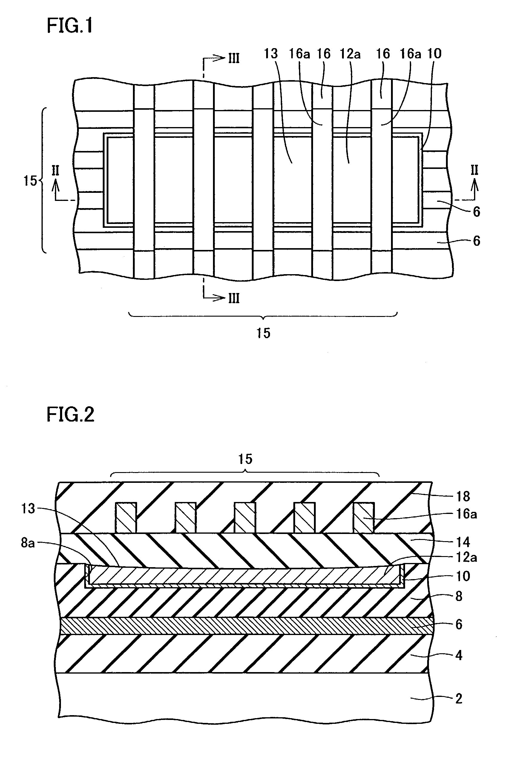
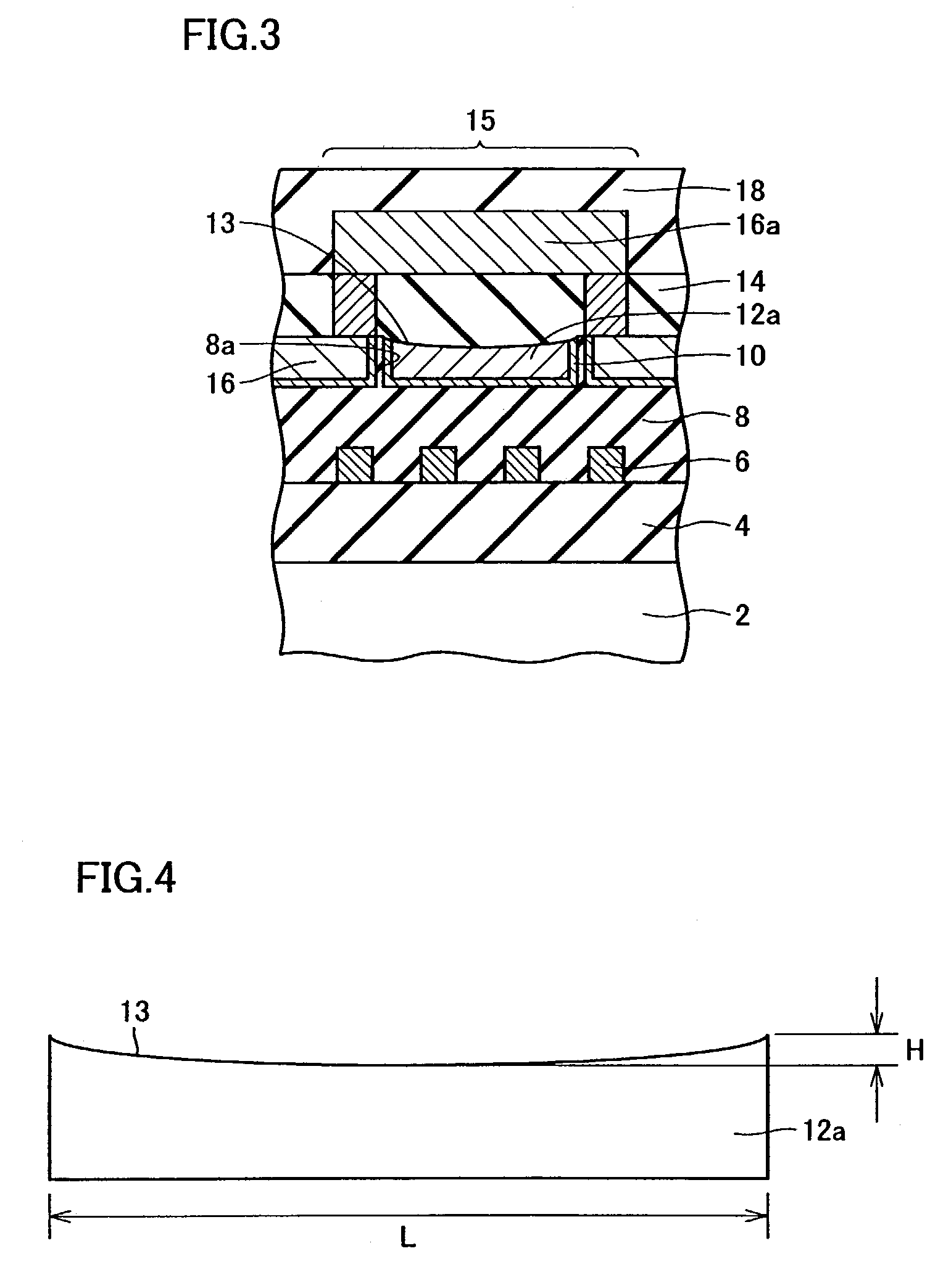
[0061]The present invention in a first embodiment provides a semiconductor device with a redundant circuit that includes a reflector layer of copper serving as a blocking layer preventing a laser beam from travelling, as described hereinafter. With reference to FIGS. 1–3, on a semiconductor substrate 2 a prescribed interconnection 6 is formed with a silicon oxide film 4 posed therebetween.

[0062]Interconnection 6 is further covered with a silicon oxide film 8 provided on silicon oxide film 4. Silicon oxide film 8 is provided with a recess 8a. In recess 8a a reflector layer of copper 12a is formed to serve as a blocking layer with a barrier metal 10 posed therebetween. The reflector layer of copper 12a is formed by damascene.

[0063]Furthermore on silicon oxide film 8 an interconnection 16 is formed to be connected to a fuse. If interconnection 16 is formed of copper, it would be formed by damascene. If it is formed for example of Al, AlCu or WSi then interconnection 16 would be formed ...

second embodiment

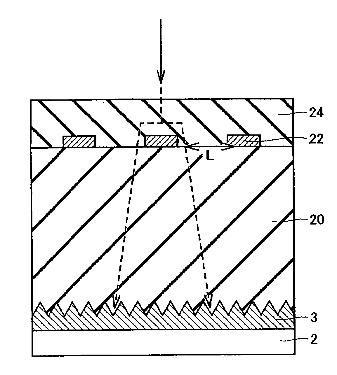
[0110]The present invention in a second embodiment provides a semiconductor device including an antireflection layer preventing reflection of a laser beam, as will be described hereinafter. With reference to FIG. 19, semiconductor substrate 2 has a surface with an antireflection layer 3 formed thereon.

[0111]Antireflection layer 3 is covered with a silicon oxide film 20. On silicon oxide film 20 a prescribed fuse 22 is formed. Fuse 22 is covered with a silicon oxide film 24 provided on silicon oxide film 20.

[0112]Antireflection layer 3 may be the exact semiconductor substrate 2 or it may be a layer formed on a surface of semiconductor substrate 2.

[0113]A laser beam is incident on antireflection layer 3 at an upper surface having depressions and protrusions formed to extend in one direction, for example as shown in FIGS. 20 and 21. Alternatively, antireflection layer 3 may have an upper surface having protrusions in a matrix, as shown in FIGS. 22 and 23.

[0114]An example of a method of...


PUM


Abstract

On a semiconductor substrate a silicon oxide film is formed and provided with a recess. In the recess a reflector layer of copper is disposed as a blocking layer with a barrier metal posed therebetween. The reflector layer of copper is covered with a silicon oxide film and thereon a fuse region provided with a plurality of fuses is provided. The reflector layer of copper has a plane of reflection recessed downward to reflect a laser beam. The reflector layer of copper is arranged to overlap substantially the entirety of the fuse region, as seen in a plane. A laser beam radiated to blow the fuse can have a reduced effect on a vicinity of the fuse region. A semiconductor device reduced in size can be obtained.

Description

BACKGROUND OF THE INVENTION[0001]1. Field of the Invention[0002]The present invention relates generally to semiconductor devices and particularly to those comprising a redundant circuit including a fuse.[0003]2. Description of the Background Art[0004]As semiconductor devices are increasingly microfabricated, foreign matters have a significant effect on yields of semiconductor devices. In semiconductor memory devices having memory cells of dynamic random access memory or the like a redundant circuit is used to connect a previously formed, spare, defectless cell in place of a specific cell defective due to foreign matters or the like.[0005]To substitute the defective cell with the defectless cell a fuse provided in the redundant circuit would be blown. The fuse is typically an interconnection layer formed in a portion corresponding to an upper layer of the semiconductor memory device.[0006]Generally a fuse is blown by laser-trimming using a laser beam. The laser beam directed to a spe...

Claims


Application Information

Patent Timeline
IPC IPC(8): H01L29/00H01L29/73H01L23/52H01L21/3205H01L21/82H01L23/525
CPCH01L23/5258H01L2924/0002H01L2924/00H01L21/82
Inventor IDO, YASUHIROKONO, KAZUSHIIWAMOTO, TAKESHI
Owner RENESAS ELECTRONICS CORP
Why Eureka
Try Eureka