Apparatus and method for transmission and remote sensing of signals from integrated circuit devices

a technology of integrated circuit devices and antennas, which is applied in the direction of voltage/current isolation, base element modifications, instruments, etc., can solve the problems of excessive power dissipation in the chip, performance and reliability of the chip, and the defect of the integrated circuit can draw significantly increased curren

Inactive Publication Date: 2006-10-03
IBM CORP
View PDF6 Cites 20 Cited by
  • Summary
  • Abstract
  • Description
  • Claims
  • Application Information

AI Technical Summary

Benefits of technology

[0006]The remote sensor is preferably a respective superconducting quantum interference device (SQUID) whose output is directed to a lock-in amplifier that is synchronized with the respective frequencies pulsing the sensed magnetic field transmitters. The present invention thus eliminates crosstalk between the individual magnetic field transmitters, noise in the form of extraneous magnetic fields, and increases the output read from each circuit under test.

Problems solved by technology

Furthermore these increased currents contribute directly to excessive power dissipation in the chip and affects, through heating, the performance and reliability of the chip.
Furthermore defective portions of integrated circuits often draw significantly increased current that can be used to identify defective portions of the integrated circuit.
However, these prior art BICS have various shortcomings that adversely impact the circuits under test for they are interactive and thus introduce parasitic resistance, additional capacitance or inductance, while consuming unproductive chip area by requiring extra inputs and outputs, additional wiring, and tester hardware to transmit the current measurement data off-chip.

Method used


Image

  • Apparatus and method for transmission and remote sensing of signals from integrated circuit devices
  • Apparatus and method for transmission and remote sensing of signals from integrated circuit devices
  • Apparatus and method for transmission and remote sensing of signals from integrated circuit devices

Examples


Embodiment Construction

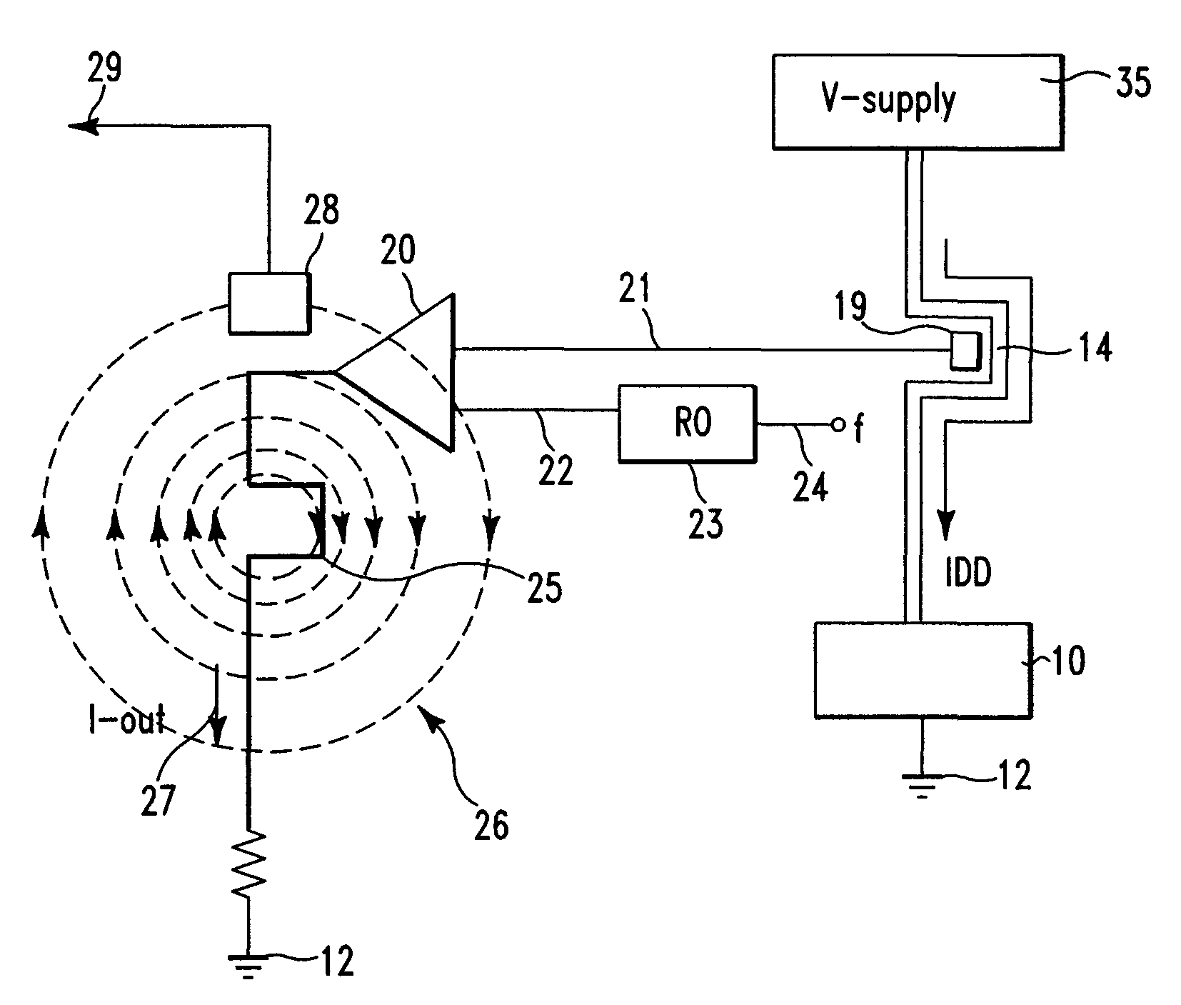
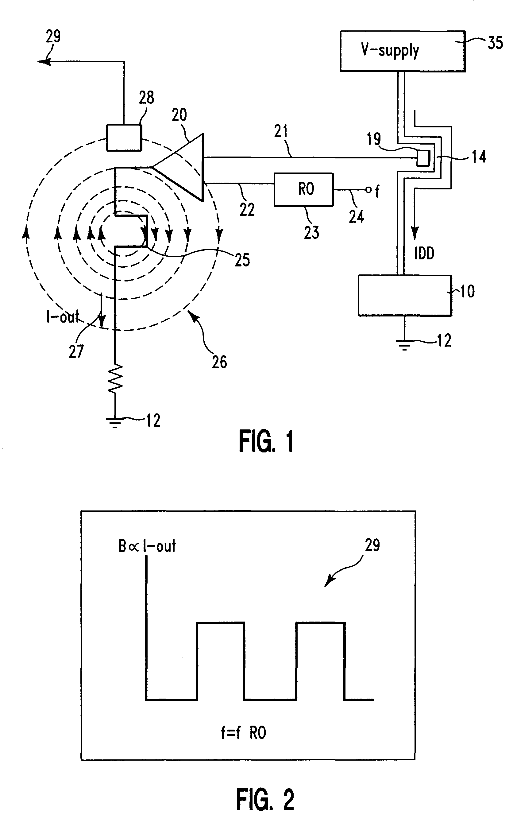
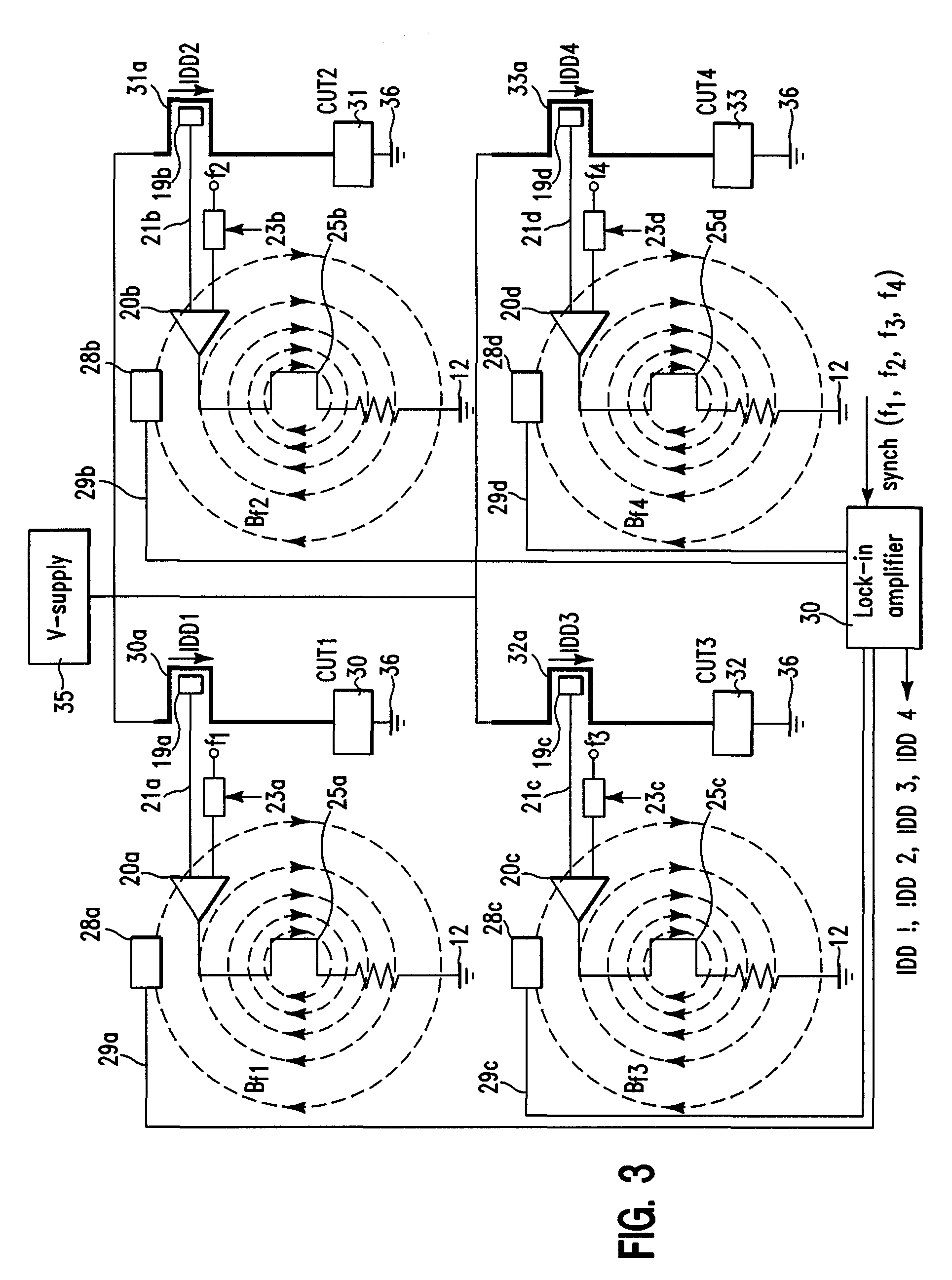
[0017]Referring now to FIGS. 1 through 6 the present invention will be described in detail, wherein: FIG. 1 is a schematic view of signal transmitter and sensor circuits of the present invention; FIG. 2 illustrates the frequency modulated magnetic field realized by the remote superconducting quantum interference device of FIG. 1; FIG. 3 schematically illustrates a chip having therein a plurality of circuits to be tested in which each circuit is provided with the present invention for determining the current in each such circuit; FIG. 4 schematically illustrates a wafer level test assembly employing the present invention; FIG. 5 illustrates the housing detail of the superconducting quantum interference device used in the wafer level test assembly of FIG. 4 and FIG. 6 illustrates a package level test assembly employing the present invention.

[0018]With reference now to the drawings and especially FIGS. 1 and 2, there is schematically shown, in FIG. 1, a circuit 10 coupled between to a ...


PUM


Abstract

An apparatus and a method for testing semiconductor devices, such as individual integrated circuits in semiconductor chips, by directing a current in each circuit through a respective selected predetermined path to establish, in each circuit, a respective focused magnetic field and converting each such magnetic field into a respective voltage which, when fed to respective amplifier gated with a respective selected frequency, will modulate each such respective voltage. Each such respective voltage is then used to create a respective pulsating magnetic field that when detected by a respective remote magnetic sensor will provide a series of respective signals representative of the current in the respective circuit from which the pulsating magnetic field was derived. By applying each such series of voltages to a lock-in amplifier synchronized at the respective frequencies gating each respective amplifier the current in each circuit being tested can be accurately determined and will be free of errors due to circuit noise or crosstalk between the circuits under test.

Description

BACKGROUND OF INVENTION[0001]The present invention relates generally to an apparatus and a method for the transmission and sensing of signals in selected portions of semiconductor integrated circuits or chips containing a plurality of individual circuits therein. More particularly, the present invention is directed to a transmission and sensing circuit arrangement especially useful in measuring currents in selected portions of semiconductor Integrated circuits.[0002]As is well known in the art, an Integrated circuit chip is comprised of a plurality of individual circuits and, as the elements forming the individual circuits in the integrated circuit chip have become smaller, each individual circuit in the chip also becomes denser causing an exponential increase especially in standby or quiescent currents in the chip and in each such individual circuit. Furthermore these increased currents contribute directly to excessive power dissipation in the chip and affects, through heating, the...

Claims


Application Information

Patent Timeline
Patent Type & Authority Patents(United States)
IPC IPC(8): G01R15/20G01R1/20G01R15/18G01R33/02
CPCG01R31/2886G01R15/20G01R31/3004G01R31/3025
Inventor LEVIN, THEODORE M.VALLETT, DAVID P.
Owner IBM CORP
Why Eureka
Try Eureka