Display panel, production method thereof and display device

A technology for a display panel and a manufacturing method, which is applied to the manufacturing of semiconductor/solid-state devices, instruments, semiconductor devices, etc., can solve the problems of increasing the manufacturing cost of the display panel, increasing the number of masks used and processes, etc., so as to reduce the manufacturing cost and reduce the The effect of using the quantity and simplifying the production process

Active Publication Date: 2014-04-16
HEFEI BOE OPTOELECTRONICS TECH +1
View PDF7 Cites 14 Cited by
  • Summary
  • Abstract
  • Description
  • Claims
  • Application Information

AI Technical Summary

Problems solved by technology

The inventors have found that using the above method to eliminate crosstalk requires an additional patterning process to form a pattern including the common electrode 11' between the pixe

Method used


Image

  • Display panel, production method thereof and display device
  • Display panel, production method thereof and display device
  • Display panel, production method thereof and display device

Examples


Example Embodiment

[0064] Example one

[0065] The embodiment of the present invention provides a display panel, which can reduce the manufacturing cost of the display panel on the premise of eliminating the crosstalk phenomenon. The display panel provided by the embodiment of the present invention will be described in detail below with reference to the accompanying drawings.

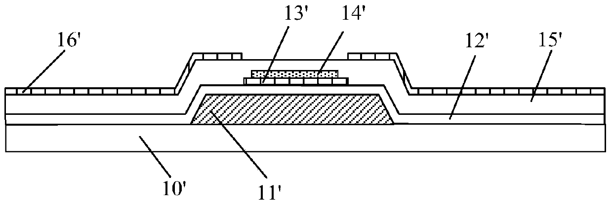
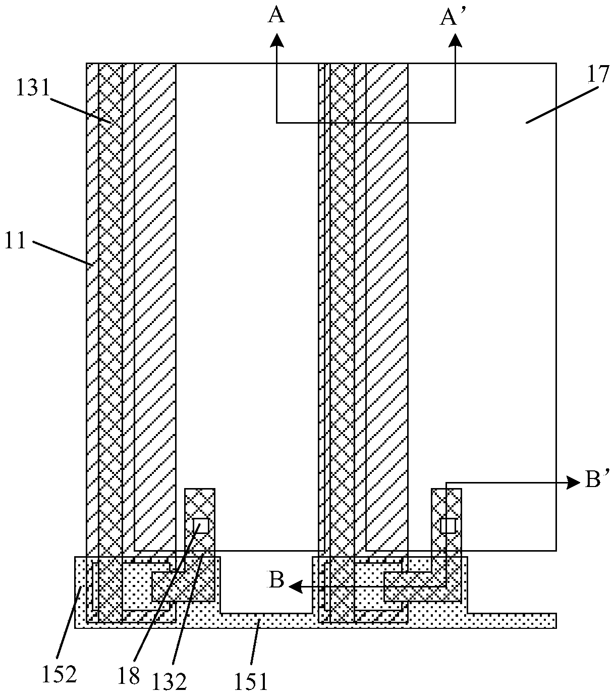
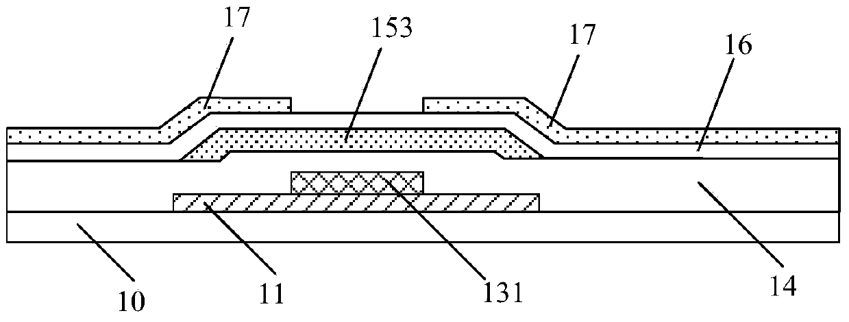
[0066] The display panel includes an array substrate, such as figure 2 , image 3 with Figure 4 As shown, the array substrate includes a plurality of film layers sequentially formed on the first base substrate 10, wherein the data line 131 and the drain electrode 132 are located in the same film layer, and the gate line 151, the gate electrode 152 and the first common electrode 153 are located in the same film layer. In the same film layer, the film layer where the gate line 151, the gate electrode 152 and the first common electrode 153 are located is located between the film layer where the data line 131 and the drain elect...

Example Embodiment

[0085] Example two

[0086] In order to prepare a display panel with the above structure, an embodiment of the present invention also provides a method for manufacturing a display panel, such as Figure 7 As shown, the manufacturing method of the display panel includes the following steps:

[0087] Step S701, forming a first metal layer on the substrate, and forming a pattern including a data line and a drain electrode through a patterning process.

[0088] First, the first metal layer is formed on the substrate by sputtering or thermal evaporation. Generally, the first metal layer is deposited by using metals such as Cr, W, Ti, Ta, Mo, Al, Cu, and their alloys. The thickness of a metal layer is

[0089] Then, coat photoresist on the first metal layer, use a mask with patterns including data lines 131 and drain electrodes 132 to cover the first metal layer coated with photoresist, and go through exposure, development, etching, etc. After the step, a pattern including the data line 1...


PUM

PropertyMeasurementUnit
Thicknessaaaaaaaaaa

Abstract

An embodiment of the invention discloses a display panel, a production method thereof and a display device, and relates to the technical field of display. Production cost of the display panel can be reduced on the premise of crosstalk elimination. The display panel comprises an array substrate. The array substrate comprises a plurality of film layers sequentially formed on a first substrate. A data line and a drain electrode are positioned on the same film layer. A grid line, a grid electrode and a first common electrode are positioned on the same film layer. The film layer where the grid line, the grid electrode and the first common electrode are positioned is positioned between the film layer where the data line and the drain electrode are positioned and the film layer where a pixel electrode is positioned.

Description

Technical field [0001] The present invention relates to the field of display technology, in particular to a display panel, a manufacturing method thereof, and a display device. Background technique [0002] The display panel in the liquid crystal display is used to display pictures, and the display panel mainly includes an array substrate and a color film substrate. Among them, the array substrate is composed of a base substrate and a plurality of film layers formed on the base substrate. [0003] figure 1 It is a cross-sectional view of the data line portion on the array substrate. A common electrode 11', a gate insulating layer 12', an active layer 13', a data line 14', and a passivation layer 15' are sequentially formed on the base substrate 10' 和Pixel electrode 16'. Wherein, the common electrode 11' is located on the same film layer as the gate line and the gate on the array substrate, that is, the common electrode 11', the gate line and the gate are simultaneously formed on t...

Claims


Application Information

Patent Timeline
IPC IPC(8): G02F1/136G02F1/1362G02F1/1368G02F1/1335G02F1/1333H01L27/12H01L21/77
Inventor 薛伟李小和邵贤杰董职福张晓洁
Owner HEFEI BOE OPTOELECTRONICS TECH
Why Eureka
Try Eureka