

Non-volatile semiconductor storage device performing ROM read operation upon power-on
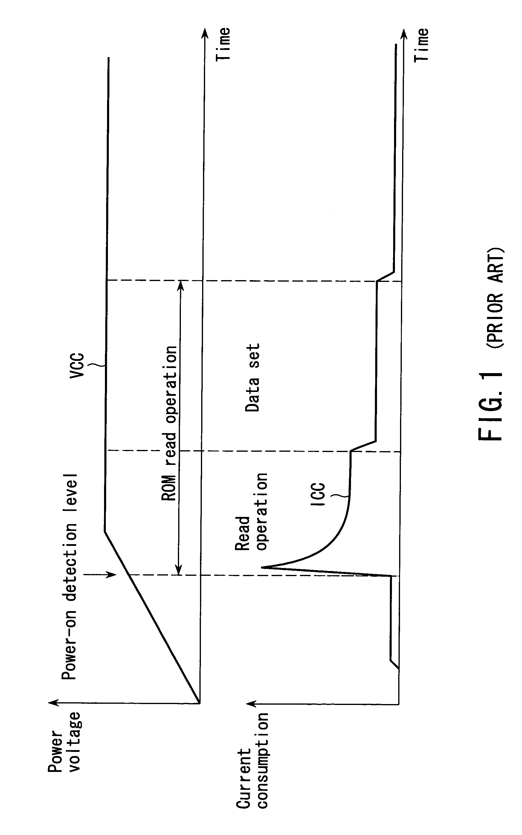
a semiconductor storage device and non-volatile technology, applied in semiconductor devices, digital storage, instruments, etc., can solve the problem of large current consumption immediately after power-on
- Summary
- Abstract
- Description
- Claims
- Application Information
AI Technical Summary
Benefits of technology
Problems solved by technology
Method used
Image

Examples
first embodiment
(First Embodiment)
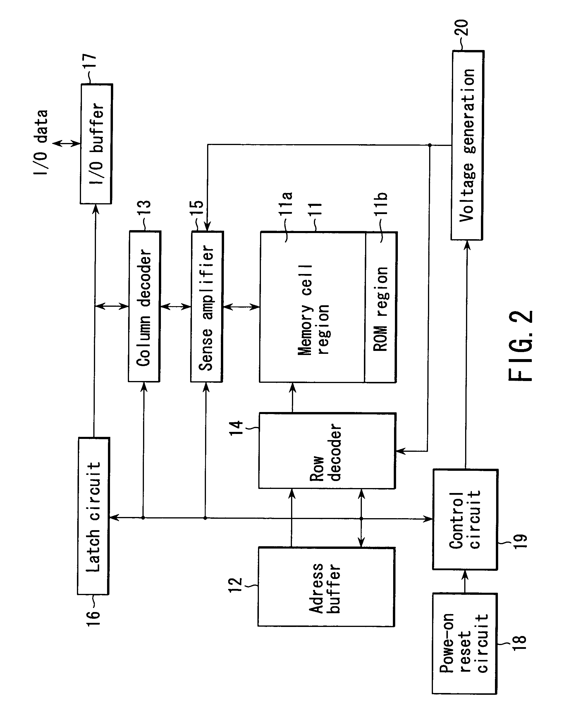
[0040]FIG. 2 is a block diagram showing the internal configuration of a non-volatile memory chip according to a first embodiment. This figure shows the internal configuration of one memory chip in a non-volatile memory configured, for example, to accommodate a plurality of, e.g. four memory chips in the same package as shown in FIG. 3. Further, this figure shows a NAND flash memory chip.
[0041]Each chip is provided with a memory cell array 11, an address buffer 12, a column decoder 13, a row decoder 14, a sense amplifier 15, a latch circuit 16, an I / O buffer 17, a power-on reset circuit 18, a control circuit 19, a voltage generating circuit 20, and other circuits.
[0042]The memory cell array 11 has not only an ordinary memory cell region 11a that stores data but also a ROM region 11b that stores various data (fuse data) that must be read after power-on, such as replacement data used to replace defective cells present in the memory cell array 11 with other redundancy ...
second embodiment
(Second Embodiment)
[0093]Now, a second embodiment of the present invention will be described.
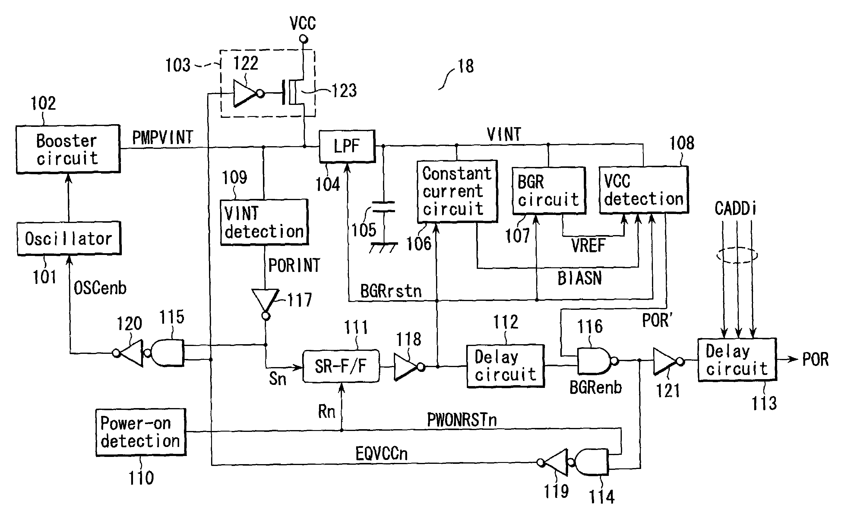
[0094]FIG. 12 shows a detailed configuration of the power-on reset circuit 18 in FIG. 1. This power-on reset circuit includes a circuit that uses the power voltage VCC as a power supply, and a circuit that uses as a power supply a boosted voltage VINT obtained by boosting the power voltage VCC.
[0095]An oscillating circuit (oscillator) 101, a booster circuit 102, a VINT-VCC short circuit 103, and other circuits operate using the power voltage VCC as a power supply.
[0096]The booster circuit 102 outputs a boosted voltage PMPVINT higher than the power voltage VCC. A low pass filter (LPF) 104 and a boosted voltage stabilizing capacitance 105 are provided at an output of the booster circuit 102.
[0097]The low pass filter 104 is composed of, for example, a resistor and a capacitor to hinder fluctuations in the potential of the boosted voltage PMPVINT to smooth this voltage.
[0098]The capacitance 105 ...
third embodiment
(Third Embodiment)
[0115]Now, a third embodiment of the present invention will be described.
[0116]FIG. 13 shows a detailed configuration of the power-on reset circuit 18 in FIG. 2. The configuration of this power-on reset circuit differs only partly from that shown in FIG. 12. Thus, only this difference will be described, and description of points corresponding to FIG. 12 is omitted.
[0117]In the power-on reset circuit shown in FIG. 12, the delay time in the delay circuit 113 is varied depending on the chip address CADDi. However, in this embodiment, the delay time in the delay circuit 112, which delays the signal BGRrstn, is varied depending on the chip address CADDi.
[0118]With this configuration, even if the VCC detecting circuit 108 detects the voltage VCC to clear the reset state of the power-on reset signal POR′, the output signal from the NAND gate 116 does not change to the “H” level unless the output signal BGRenb from the delay circuit 112 changes to the “H” level.
[0119]That ...
PUM
 Abstract
Description
Claims
Application Information