Semiconductor device and method for manufacturing the same

a technology of semiconductor devices and ring rings, which is applied in the direction of semiconductor devices, semiconductor/solid-state device details, electrical equipment, etc., can solve the problems of limited wiring materials, method is not applicable to multi-layer wiring structures, and limit, so as to prevent moisture from entering the upper layer and enhance the adhesion between the upper end portion of the first barrier metal film and the upper layer

Inactive Publication Date: 2006-10-10
FUJITSU SEMICON LTD
View PDF19 Cites 25 Cited by
  • Summary
  • Abstract
  • Description
  • Claims
  • Application Information

AI Technical Summary

Benefits of technology

[0023]The present invention is therefore made in consideration of the above-described situation, and its object is to provide a semiconductor device which can prevent cracks and suitably intercept entry of moisture or the like as well, and a method for manufacturing the same.
[0026]As described above, the semiconductor device of the present invention and the semiconductor device manufactured by the method for manufacturing a semiconductor device of the present invention, are configured such that the barrier metal bottom face portion, covering the bottom face of the via contact portion, of the second barrier metal film is in contact with at least a portion of the upper end portion of the first barrier metal film. Therefore, according to the present invention, the adhesiveness between the upper end portion of the first barrier metal film and an upper layer is enhanced to enable prevention of entry of moisture or the like at a connecting portion, as a boundary, between the upper end portion of the first barrier metal film and the barrier metal bottom face portion. This can solve problems that the first conductor pattern formed inside the first barrier metal film is corroded and the like.

Problems solved by technology

In semiconductor devices in recent years, with miniaturization and high integration, the design rule becomes smaller every year, giving rise to a technical limit in a method of forming a metal wiring material by direct etching.
For employment of this method, however, the wiring material is limited to a material such as Al—Cu capable of being etched.
This method is not applicable to a multilayer wiring structure including Cu wiring patterns which need to be formed by the damascene method.
The insulation film, however, has poor adhesiveness with a metal film in use for the wiring pattern 41.
This causes a problem that the insulation film cannot prevent cracks at the interface between the insulation film and the wiring pattern 41 nor secure moistureproofness when moisture or the like enters.
Cu, however, is hard to be patterned by etching, and thus the method shown in FIG. 3 is not applicable as described above.

Method used


Image

  • Semiconductor device and method for manufacturing the same
  • Semiconductor device and method for manufacturing the same
  • Semiconductor device and method for manufacturing the same

Examples


first embodiment

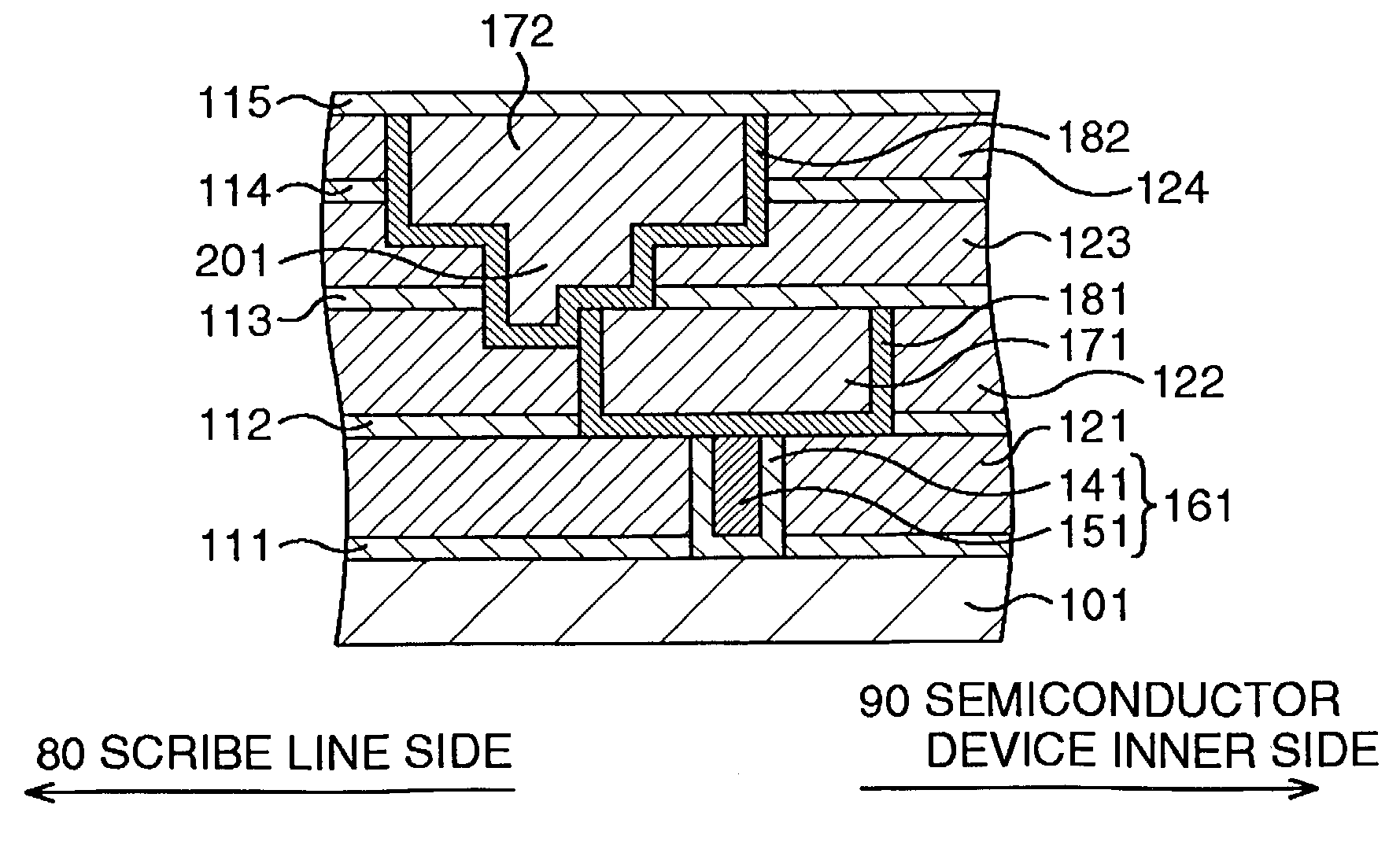
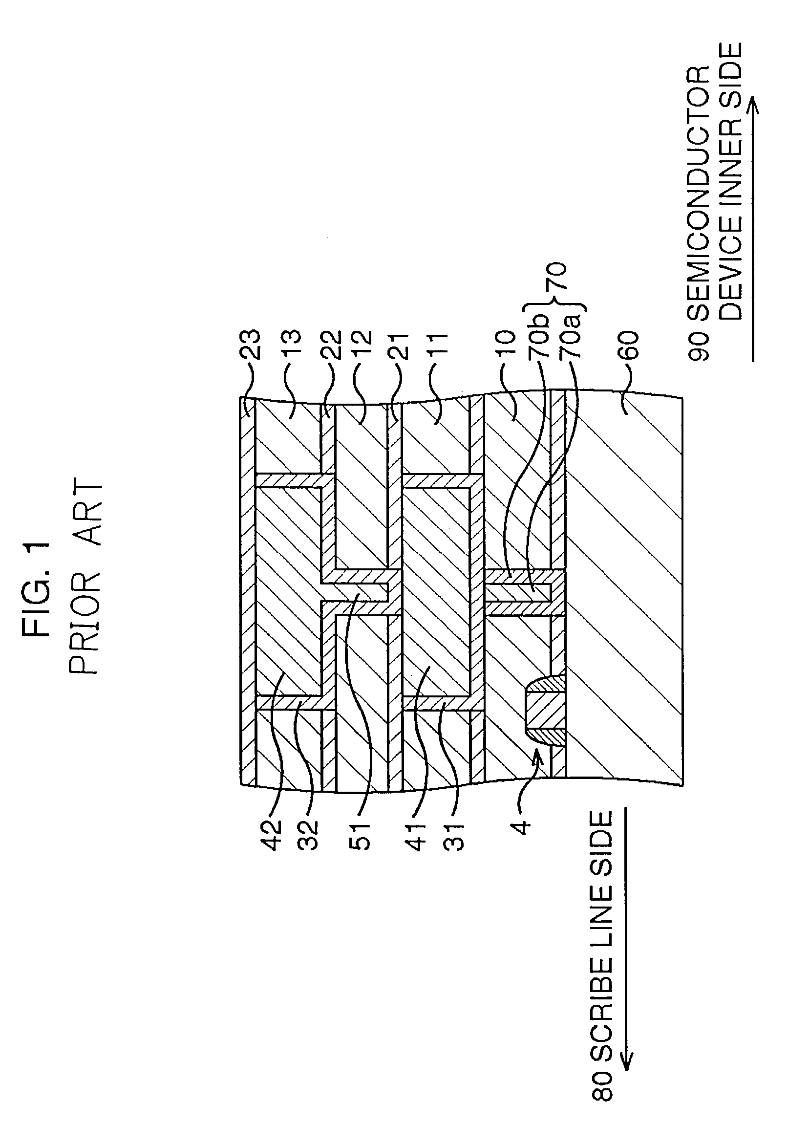
[0059]FIG. 4A to FIG. 15B show steps of manufacturing a moisture-proof ring according to a first embodiment of the present invention when a dual damascene method is used. In the drawings, the left-hand side is a scribe line side 80, and the right-hand side is a semiconductor device inner side 90. Pointing a wall will show the whole space like a resist window 131a in FIG. 4A.

Step of Patterning Photoresist Film for Forming Contact

[0060]Referring to FIG. 4A, after formation of a not-shown circuit element on a semiconductor substrate 101, a silicon nitride film 111 and a silicon oxide film 121 are formed on and above the semiconductor substrate 101 to have thicknesses of 100 nm and 900 nm, respectively. To flatten the circuit element portion, the silicon oxide film 121 is polished using a CMP method so that the silicon oxide film 121 is formed to have a thickness of 600 nm. On the silicon oxide film 121, a photoresist film 131 is then applied, exposed to light, and further developed to ...

second embodiment

[0089]FIG. 16A to FIG. 17 show steps of manufacturing a semiconductor device according to a second embodiment of the present invention. In the drawings, the same reference numbers are assigned to portions corresponding to the previously described portions, and the description thereof is omitted.

Step of Etching Silicon Oxide Film for Forming Wiring

[0090]Referring to FIG. 16A, in this embodiment, after the formation of the structure shown in FIG. 13, the silicon nitride film 114 under the opening 124b in the silicon oxide film 124 and the silicon nitride film 113 under the opening 123a in the silicon oxide film 123 are etched under the condition that no overetching is performed.

[0091]As a result, as shown in FIG. 16A, the shape of the opening 124b is transferred, with the silicon oxide film 124 as a mask, to the silicon nitride film 114 to form an opening 114b. Concurrently, the silicon nitride film 113 is also etched with the silicon oxide film123 as a mask, so that the shape of the ...

third embodiment

[0097]FIG. 18A to FIG. 20 show steps of manufacturing a semiconductor device according to a third embodiment of the present invention. In the drawings, the same reference numbers are assigned to the previously described portions, and the description thereof is omitted.

Step of Patterning Photoresist Film for Forming Via Pattern

[0098]Referring to FIG. 18A, in this embodiment, a silicon nitride film 113, a silicon oxide film 123, a silicon nitride film 114, and a silicon oxide film 124 are formed on and above a wiring pattern 171 to have thicknesses of 70 nm, 650 nm, 70 nm, and 500 nm, respectively. On the silicon oxide film 124, a photoresist film 133 is applied, exposed to light, and further developed to form a photoresist window 133a which corresponds to a via pattern.

[0099]It should be noted that the photoresist window 133a is formed in such a manner that a first outer peripheral portion 205, covering a sidewall face on the outer peripheral side of a Cu film 191 being the wiring pa...


PUM


Abstract

After formation of a contact pattern on a semiconductor substrate, a first wiring pattern composed of a first barrier metal film and a first conductor pattern is formed on the contact pattern. A moisture-proof ring is formed which has such a structure that an outer peripheral portion, covering a sidewall face on the outer peripheral side of the first conductor pattern, of the first barrier metal film, is in contact at the upper end portion with a barrier metal bottom face portion, covering the bottom face of a via contact portion, of a second barrier metal film. This results in formation of a barrier metal film such as Ta, TiN, or the like, with no discontinuation, in the whole region from the semiconductor substrate to an silicon oxide film being the uppermost layer, thereby improving adhesiveness for prevention of cracks and entry of moisture.

Description

CROSS-REFERENCE TO RELATED APPLICATIONS[0001]This application is based upon and claims the benefit of priority from the prior Japanese Patent Application Nos. 2002-165818, filed on Jun. 6, 2002 and 2003-076962, filed on Mar. 20, 2003, the entire contents of which are incorporated herein by reference.BACKGROUND OF THE INVENTION[0002]1. Field of the Invention[0003]The present invention generally relates to a semiconductor device and a method for manufacturing the same and, more specifically, to a semiconductor device with a moisture-proof ring and a method for manufacturing the same.[0004]2. Description of the Related Art[0005]In semiconductor devices in recent years, with miniaturizatation and high integration, a multilayer wiring structure, in which a plurality of interlayer insulation films are layered in each of which a wiring pattern is embedded, is often used to connect many semiconductor elements to each other on a common substrate. In such a semiconductor device, moisture or c...

Claims


Application Information

Patent Timeline
Patent Type & Authority Patents(United States)
IPC IPC(8): H01L21/302H01L21/461H01L21/3205H01L21/768H01L23/00H01L23/522H01L23/532
CPCH01L21/76802H01L21/76808H01L21/76813H01L21/76838H01L21/76843H01L21/76847H01L23/53238H01L23/564H01L21/76852H01L2924/0002H01L2221/1036H01L2924/00H01L21/768
Inventor WATANABE, KENICHIKAWANO, MICHIARI
Owner FUJITSU SEMICON LTD
Why Eureka
Try Eureka