
Integrated circuit with enhanced coupling

a technology of integrated circuits and couplings, applied in the direction of near-field systems using receivers, instruments, burglar alarm mechanical actuation, etc., can solve the problems of increasing the cost of conventional passive rfid tags for dominant use. , to achieve the effect of optimizing the coupling efficiency and increasing the coupling efficiency

Inactive Publication Date: 2006-10-10
CELIS SEMICONDUCTOR CORP
View PDF4 Cites 185 Cited by
  • Summary
  • Abstract
  • Description
  • Claims
  • Application Information

AI Technical Summary

Benefits of technology

[0023]One advantage of the present invention is that the present invention utilizes IC 2 in which all components of integral resonant circuit 6 are formed as an integral part of the integrated circuit process, thereby taking advantage of no wire bond pads, while extending the read distance.

Problems solved by technology

Nevertheless, conventional RFID technology is too expensive for dominant use in such applications.
However, passive field powered RFID tags require at least an order of magnitude more power in the interrogation signal from the base station than an active RFID tag.
Even conventional passive RFID tags are too expensive for dominant use in applications dominated by bar codes today.
A major factor driving up fabrication costs of RFID tags is the size of the silicon integrated circuit that makes up the tag.
Since RFID tag chips are generally relatively small compared to the size of a bond pad, these bond pads consume a significant percentage of the integrated circuit area of a conventional RFID tag.
However, since such integrated antennas are form-factor constrained and are necessarily small, the coupling efficiency to the radiated field substantially reduced in RFID tags with an internal antenna.
Consequently, this method often results in exceedingly short operating read distances from the base station.
However, maximum levels permissible are limited by government regulation.

Method used


Image

  • Integrated circuit with enhanced coupling
  • Integrated circuit with enhanced coupling

Examples


Embodiment Construction

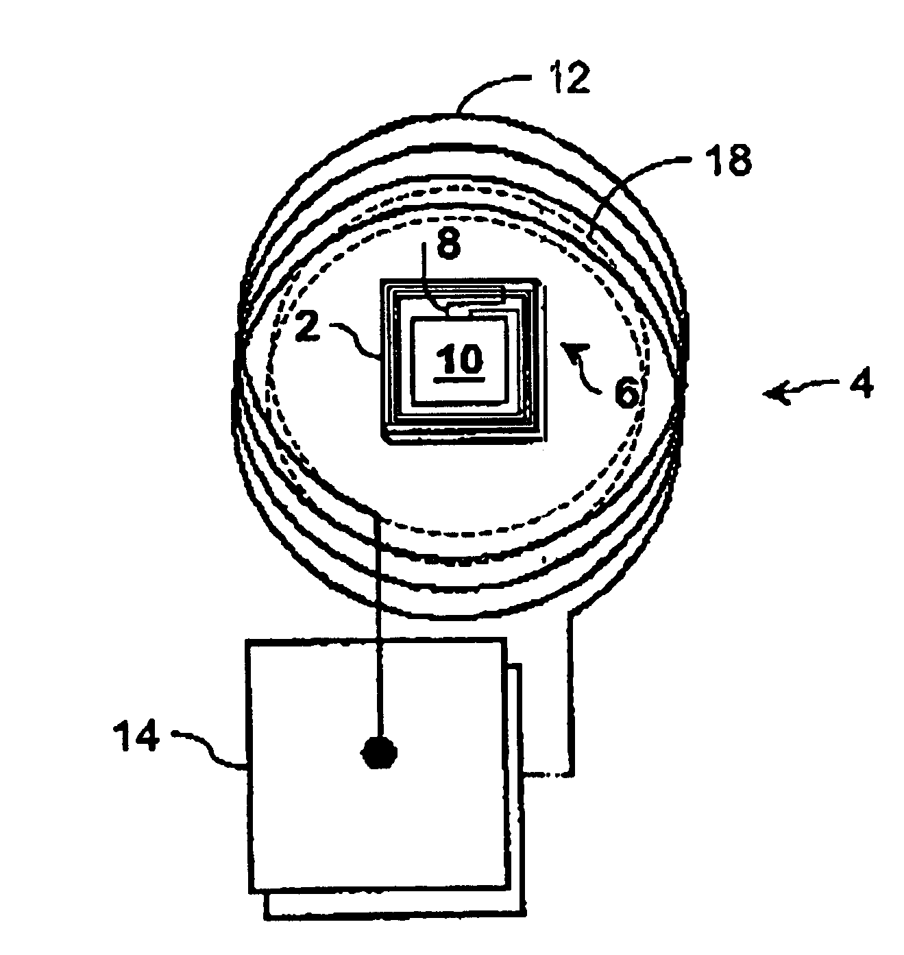
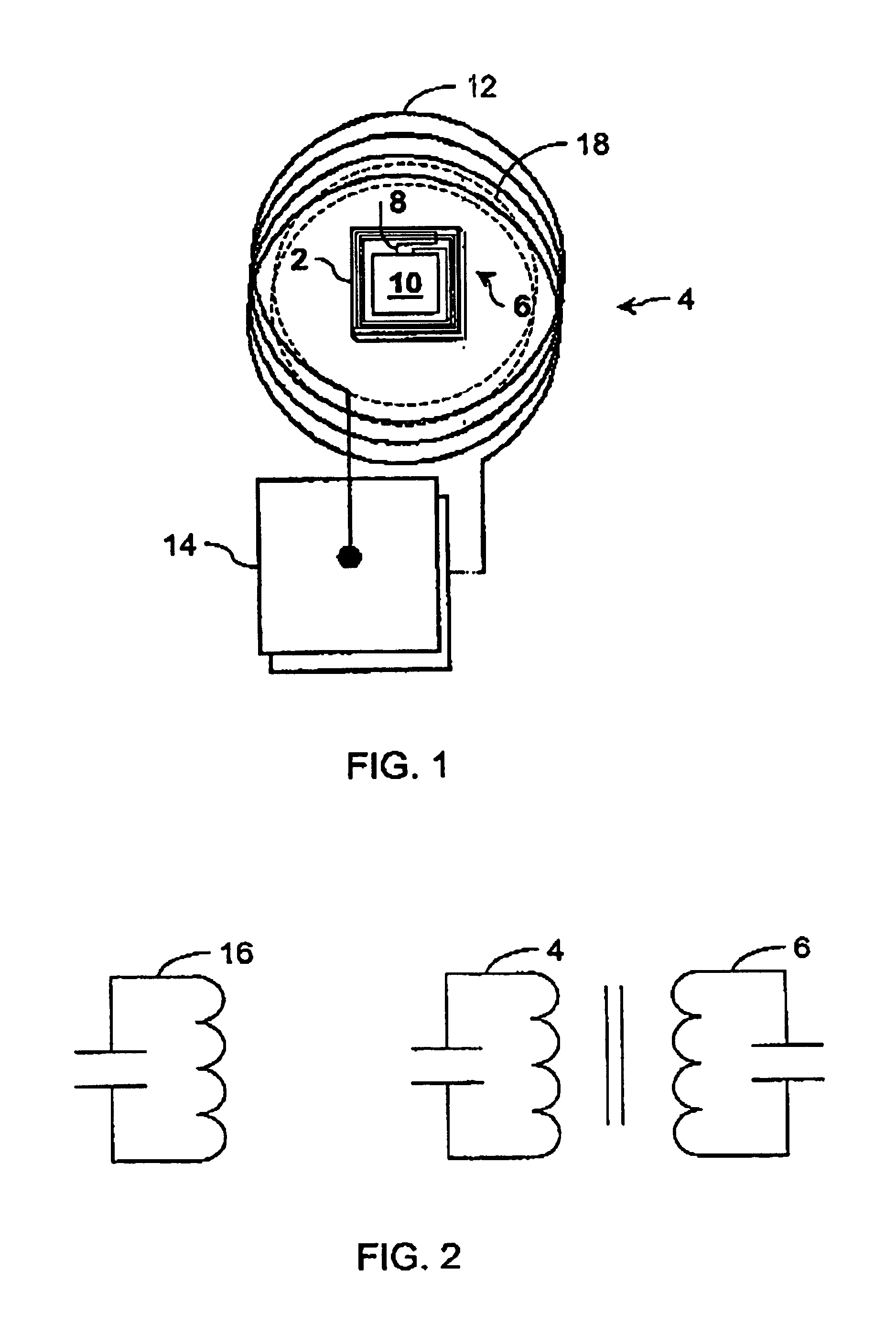
[0012]FIG. 1 illustrates one embodiment of the present invention system for conveying a radio frequency (RF) signal to an integrated circuit (IC). In one embodiment, the RF signal is generated by a base station (not shown). Alternatively, the RF signal is generated by any device for communicating with the IC.

[0013]The system includes IC 2 and intermediate resonant circuit 4. IC 2 and intermediate resonant circuit 4 are affixed proximate one another. The proximity is selected based on the characteristics of the IC 2, intermediate resonant circuit 4, and the RF signal.

[0014]IC 2 is an integrated circuit device for performing any desired function. IC 2 includes integral resonant circuit 6 and integrated circuitry (not shown) necessary for performing the desired function. In one embodiment, IC 2 is an RFID tag.

[0015]Integral resonant circuit 6 is any component or combination of components configured to resonate in response to an RF signal and to provide an electrical signal to the integ...


PUM


Abstract

A system for conveying a radio frequency (RF) signal from a base station to a detached integrated circuit (IC) has an intermediate resonant circuit and an IC. The intermediate resonant circuit is configured to resonate in response to the RF signal from the base station, reproducing the RF signal. The IC has an integral resonant circuit configured to resonate in response to the reproduced RF signal. The IC and the intermediate resonant circuit are affixed proximate each other. Both are separate from the base station and each other. Either or both of the intermediate resonant circuit and the integral resonant circuit may contact a high magnetic permeability layer. The intermediate resonant circuit may be formed of conductive ink.

Description

FIELD OF THE INVENTION[0001]This invention relates in general to signal coupling enhancement, and more particularly, to a system for relaying a signal to an integrated circuit.BACKGROUND OF THE INVENTION[0002]Radio Frequency Identification (RFID) transponders (tags) are generally used in conjunction with an RFID base station, typically in applications such as inventory control, security, access cards, and personal identification. The base station transmits a carrier signal that powers circuitry in the RFID tag when it is brought within a read range of the base station. Data communication between the tag and the station is achieved by modulating the amplitude of the carrier signal with a binary data pattern, usually amplitude shift keying. To that end, RFID tags are typically integrated circuits that include, among other components, antenna elements for coupling the radiated field, rectifiers to convert the AC carrier signal to DC power, and demodulators to extract the data pattern f...

Claims


Application Information

Patent Timeline
IPC IPC(8): G08B13/14G06K19/07G06K7/00G08B13/24H04B1/59H04B5/02
CPCG06K7/0008G06K7/10178G06K19/07756G08B13/2414G08B13/2417G08B13/2448G06K19/07
Inventor DEVILBISS, ALAN D.
Owner CELIS SEMICONDUCTOR CORP
Learn More