Determination of center of focus by parameter variability analysis

Inactive Publication Date: 2006-10-10
NANOMETRICS
View PDF29 Cites 24 Cited by
  • Summary
  • Abstract
  • Description
  • Claims
  • Application Information

AI Technical Summary

Benefits of technology

[0038]A primary advantage of the present invention is that it permits measuring parameters relating to a lithography device without the use of optical, SEM or similar microscopy metrology tools.
[0039]Another advantage of the present invention is that it provides a method and device that permits obtaining results, including center of focus, in a lithography device, such as a stepper, in a shorter period of time and at lower cost than conventional and known methods.
[0040]Other objects, advantages and nov

Problems solved by technology

However, while SEM metrology can resolve features on the order of 0.1 microns, the process is costly, requires a high vacuum chamber, is relatively slow in operation and is difficult to automate.
Optical microscopes can be employed, but do not have the required resolving power for sub-micron structures.
However, these methods still require use of SEM, optical microscopes or similar direct measurement devices.
How

Method used


Image

  • Determination of center of focus by parameter variability analysis
  • Determination of center of focus by parameter variability analysis
  • Determination of center of focus by parameter variability analysis

Examples


Example

EXAMPLE 1

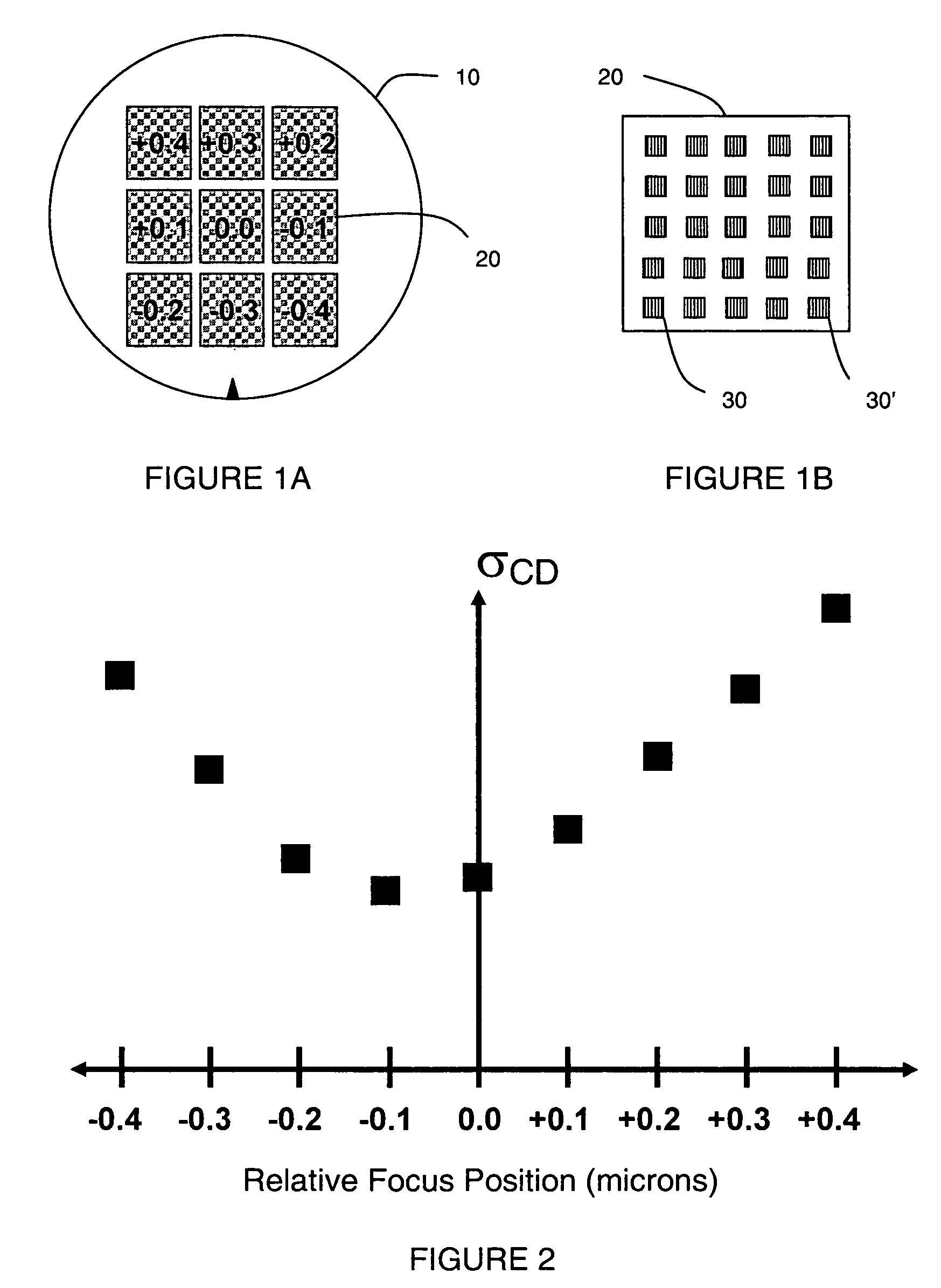
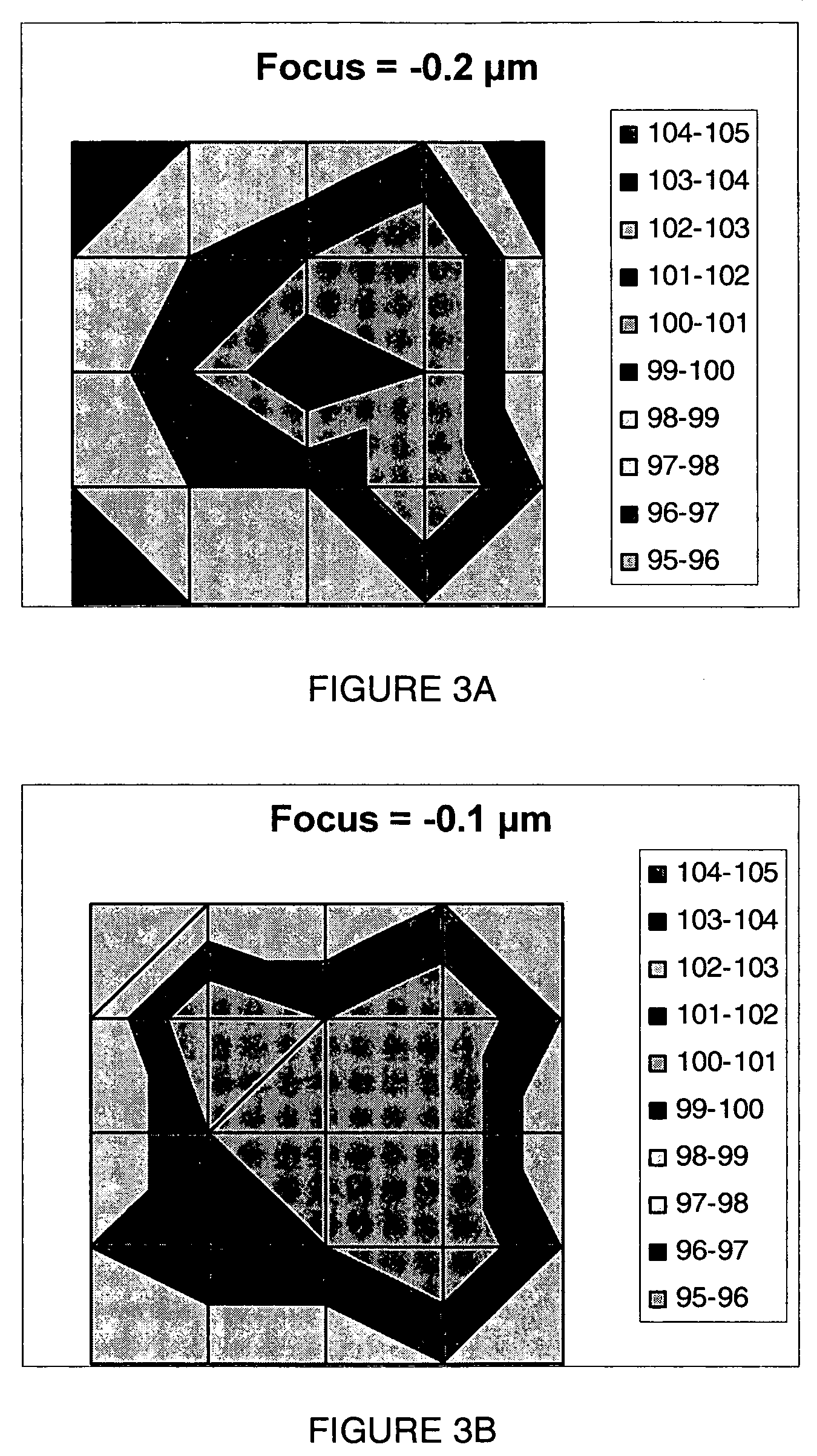
[0100]According to the present invention, five fields are exposed at different focus values, taken through focus from −0.2 microns to +0.2 microns in 0.1 micron increments. Each field contains a 5×5 array of equally spaced diffraction structures, similar to that depicted in FIG. 1B. FIGS. 3A–3E graphically display the CDs of the diffraction structures in each field. FIG. 4 is a graph of the 1-sigma standard deviation of the CDs of all 25 diffraction structures in each field. As above, best focus is achieved for the −0.1 micron focus setting.

[0101]For real time focus monitoring and process control, it is important to be able to correct for focus drift before it becomes too large. Thus it is advantageous to monitor the CD or other chosen feature of a subset of the diffraction structures which exhibit a larger variation in the chosen feature than the variation of all 25 diffraction structures in each field. For example, chosen features of diffraction structures located in the ...

Example

EXAMPLE 2

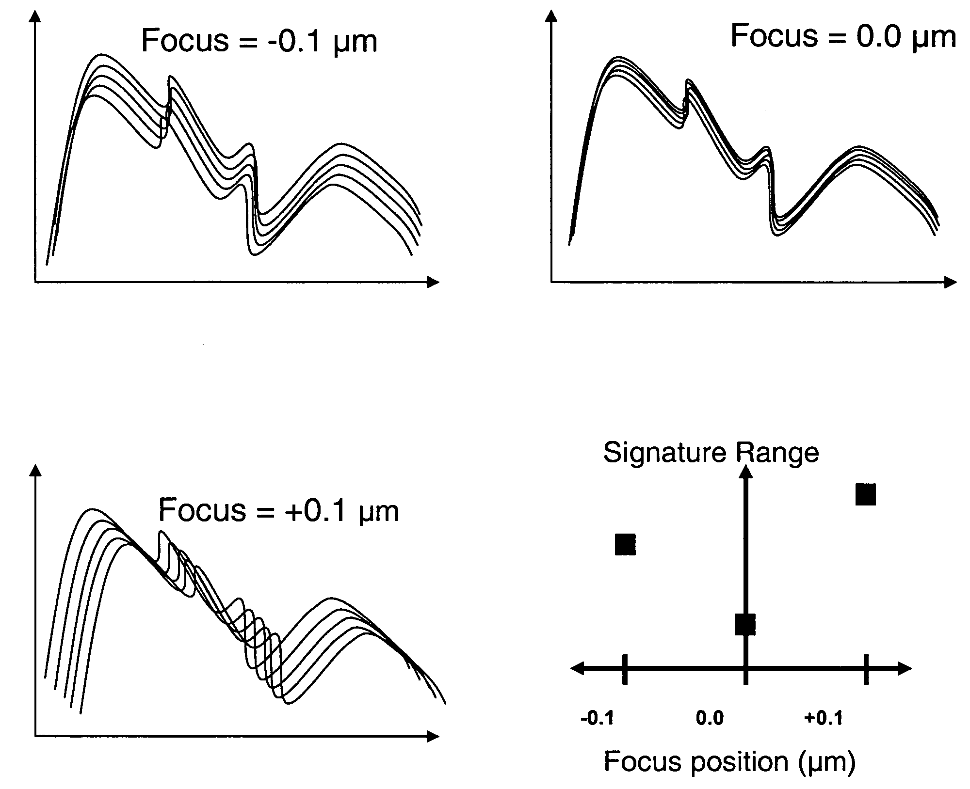
[0103]According to the second preferred embodiment discussed above, FIG. 7 depicts the diffraction signatures arising from five spaced diffraction structures within each of three fields shot at different focus values. In this example it is easily determined by inspection that the variation in signatures is minimum for the field shot at the 0.0 micron focus point. The graph in FIG. 7 plots the range, or spread, of the signature intensities for each field. As expected, the minimum value is for the field shot at 0.0 focus, which field is at best focus. This method may be substituted for the embodiment described above for all purposes, including those of process control and focus drift monitoring.

Example

EXAMPLE 3

[0104]A typical process control application involves monitoring the variation over time of the chosen feature as multiple wafers printed with the same mask and using the same process are manufactured. FIG. 8 depicts variation of the chosen feature (in this case, variation of CD measured as the 3-sigma of measurements, preferably across the illumination field previously determined according to the methods of the present invention to be at center of focus) measured at one hour intervals. Because the same diffraction structures in the same field are measured for each wafer, and each wafer is printed with the same mask and process, the variability should be the same for each wafer. However, the focus of the lithography tool may drift with time, which leads to higher CD variation, as shown in FIG. 8. Based on prior knowledge an acceptable amount of variation for process control might be 2.4 nm. Hence, a control limit of 2.4 nm is shown in FIG. 8 with a dashed line. Variation wit...


PUM


Abstract

Methods for the determination of center of focus and process control for a lithographic tool. Diffraction signatures are obtained from a plurality of diffraction structures located within multiple different focus setting fields. Variability of diffraction signatures with each field are determined, by direct analysis or comparison to a library. The variation or uniformity may be represented by any measure, including the standard deviation or the range of values of a chosen feature of a library of theoretical diffraction structures or the variability or uniformity of the diffraction signatures themselves, such as by RMS difference or intensity range. The methods may be used for process control and monitoring of focus drift by determining intra-field variation of diffraction signatures of multiple diffraction structures in a series of wafers.

Description

CROSS-REFERENCE TO RELATED APPLICATION[0001]This application claims the benefit of the filing of U.S. Provisional Patent Application Ser. No. 60 / 462,353, entitled Determination Of Center Of Focus In Lithographic Applications, filed on Apr. 10, 2003, the specification of which is incorporated herein by reference.BACKGROUND OF THE INVENTION[0002]1. Field of the Invention (Technical Field)[0003]The present invention relates to methods for determination of parameters in lithography devices and applications by analysis of the variation in measurements of multiple diffracting structures located in different fields on a wafer, including determination of center of focus in lithography applications, such as for photoresist lithographic wafer processing, and methods of process and quality control using such determinations.[0004]2. Background Art[0005]Note that the following discussion refers to a number of publications by author(s) and year of publication, and that due to recent publication d...

Claims


Application Information

Patent Timeline
IPC IPC(8): G01B9/00G01B11/00G01B11/14G01B11/04G01B11/06G03B27/52G03C5/00G03FG03F7/20
CPCG01N21/4788G01N21/9501G01N21/956G03F7/70483G03F7/705G03F7/70508G03F7/70533G03F7/70641G01N2021/95615G03F7/20G03B27/52G01B9/00
Inventor LITTAU, MICHAEL E.RAYMOND, CHRISTOPHER J.
Owner NANOMETRICS
Why Eureka
Try Eureka