Patterning with rigid organic under-layer

a technology of organic underlayer and patterning layer, which is applied in the direction of basic electric elements, electrical apparatus, and semiconductor devices, can solve the problems of poor etch selectivity of traditional barc material during etching of ic material, and disadvantageous distort the patterning of the photo resist layer, so as to enhance the speed performance of an integrated circuit and avoid mechanical and etch properties

Inactive Publication Date: 2006-10-17
GLOBALFOUNDRIES INC
View PDF8 Cites 8 Cited by
  • Summary
  • Abstract
  • Description
  • Claims
  • Application Information

AI Technical Summary

Benefits of technology

[0014]In this manner, because the rigid organic under-layer has such favorable mechanical and etch properties, the rigid organic mask structure has a critical dimension that is minimized beyond that possible with the traditional BARC material. Such a further minimized critical dimension advantageously enhances the speed performance of an integrated circuit fabricated with such a rigid organic mask structure.

Problems solved by technology

Such reflection during the photolithography process would disadvantageously distort the patterning of the photo-resist layer 108.
Thus, the traditional BARC material has poor etch selectivity during etching of the IC material 102 which may be polysilicon for example.

Method used


Image

  • Patterning with rigid organic under-layer
  • Patterning with rigid organic under-layer
  • Patterning with rigid organic under-layer

Examples


Embodiment Construction

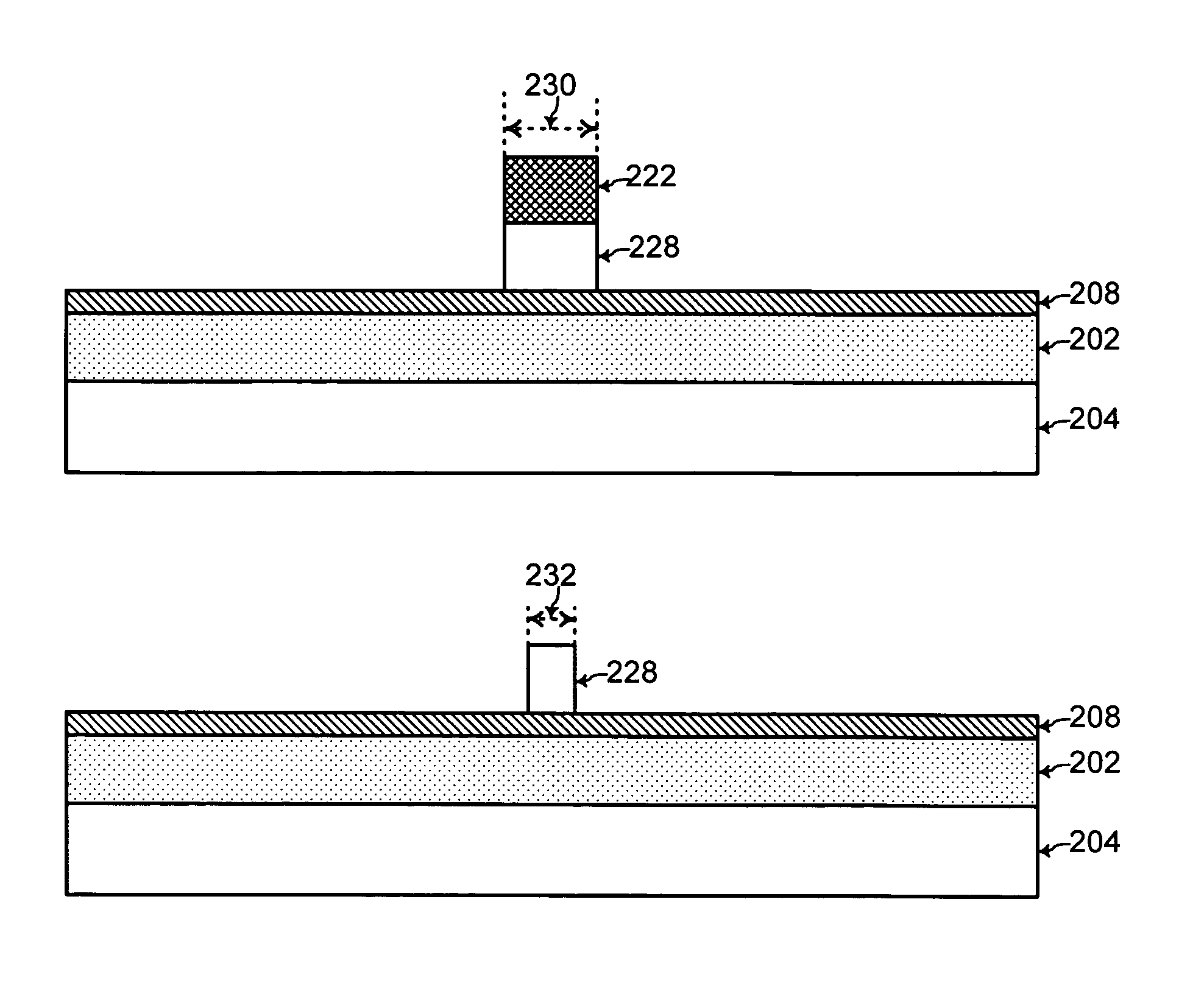
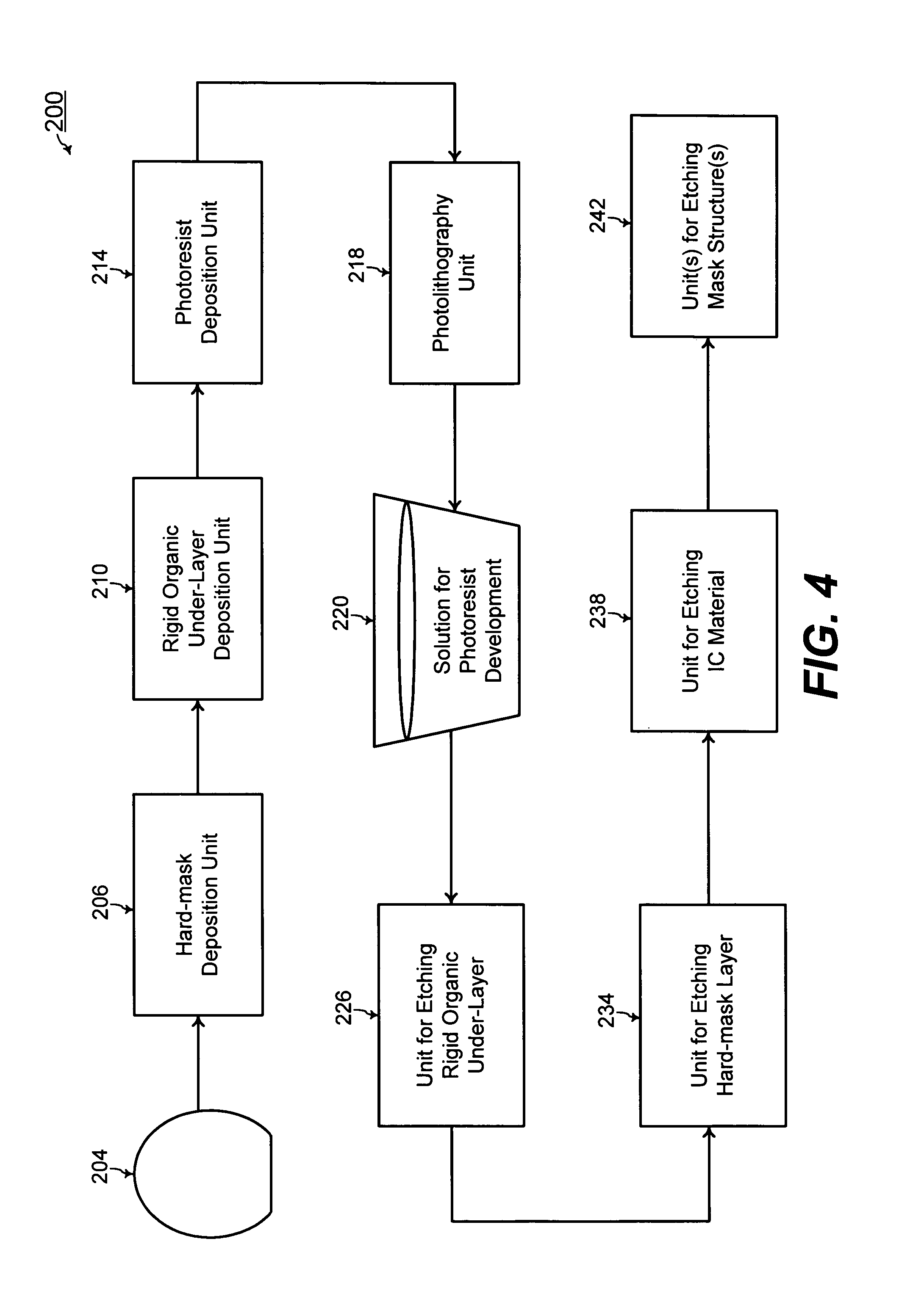
[0020]FIG. 4 illustrates a system 200 for forming mask structures with a rigid organic under-layer for patterning an IC (integrated circuit) material, according to an embodiment of the present invention. Referring to FIG. 5, an IC material 202 to be patterned is deposited on a semiconductor substrate 204. The semiconductor substrate 204 is comprised of a silicon wafer according to one embodiment of the present invention.

[0021]The IC material 202 is any material patterned for forming an integrated circuit such as polysilicon for forming a gate of a MOSFET (metal oxide semiconductor field effect transistor) for example. In that case, the IC material 202 is deposited with an example thickness range of from about 500 Å (angstroms) to about 2,500 Å, in one embodiment of the present invention. Processes for depositing IC material to be patterned in general are individually known to one of ordinary skill in the art.

[0022]Referring to FIGS. 4 and 5, the semiconductor substrate 204 having th...


PUM


Abstract

For patterning an IC (integrated circuit) material, a rigid organic under-layer is formed over the IC material, and the rigid organic under-layer is patterned to form a rigid organic mask structure. In addition, the rigid organic mask structure is trimmed to lower a critical dimension of the rigid organic mask structure beyond the limitations of traditional BARC mask structures. Any portion of the IC material not under the rigid organic mask structure is etched away to form an IC structure.

Description

TECHNICAL FIELD[0001]The present invention relates generally to integrated circuit fabrication, and more particularly, to patterning an IC (integrated circuit) material using a rigid organic under-layer for achieving critical dimensions beyond traditional photolithography limitations.BACKGROUND OF THE INVENTION[0002]Referring to FIG. 1, for patterning an IC (integrated circuit) material 102 formed on a semiconductor substrate 104, a BARC (bottom anti-reflective coating) layer 106 and a photo-resist layer 108 are formed on the IC material 102. Referring to FIGS. 1 and 2, a photolithography process is performed to pattern the photo-resist layer 108 to form a photo-resist mask structure 110 having a first critical dimension 112.[0003]Referring to FIGS. 2 and 3, any portion of the BARC layer 106 not under the photo-resist mask structure 110 is etched away to form a BARC mask structure 114. During the etching process for forming the BARC mask structure 114, the exposed portions of the ph...

Claims


Application Information

Patent Timeline
Patent Type & Authority Patents(United States)
IPC IPC(8): H01L21/3205
CPCH01L21/0337H01L21/0338H01L21/28123H01L21/32139H01L21/28035Y10S438/947Y10S438/942
Inventor LYONS, CHRISTOPHER F.PLAT, MARINA V.DAKSHINA-MURTHY, SRIKANTESWARABELL, SCOTT A.TABERY, CYRUS E.
Owner GLOBALFOUNDRIES INC
Why Eureka
Try Eureka