Controlling apparatus and controlling method of optical switching device
a technology of optical switching device and control apparatus, which is applied in the direction of instruments, optical elements, discharge tubes/lamp details, etc., can solve the problems of difficult to realize an optical switching device capable of coping with several tens or more channels, large optical loss within the optical switching device, and limitations in coping with the increase of the number of channels. to achieve the effect of reducing optical loss
- Summary
- Abstract
- Description
- Claims
- Application Information
AI Technical Summary
Benefits of technology
Problems solved by technology
Method used
Image
Examples
first embodiment
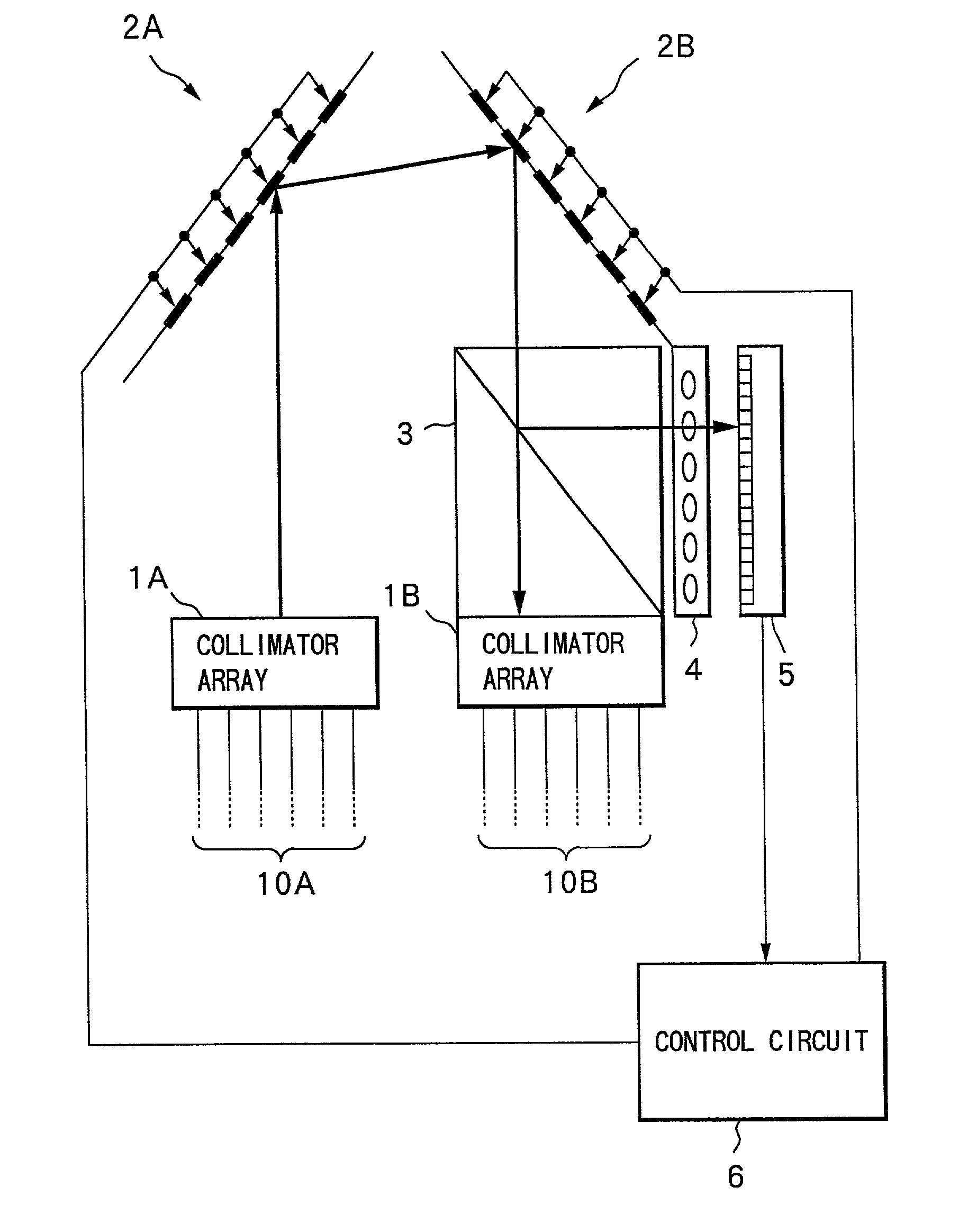
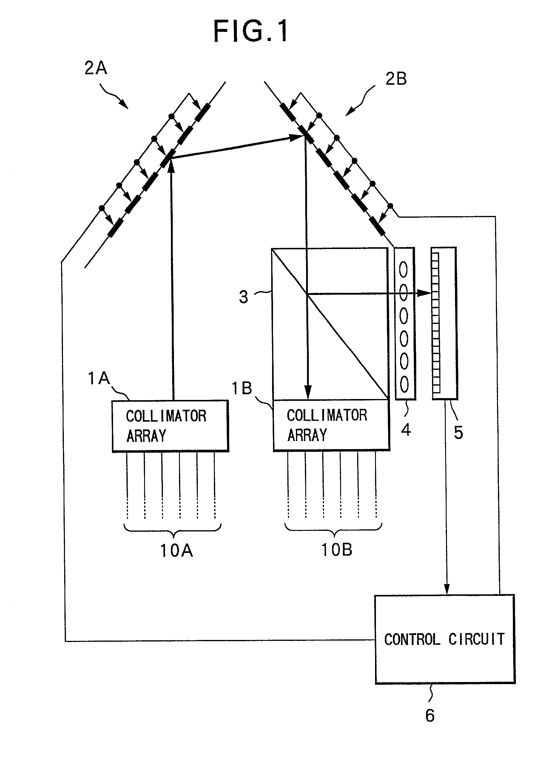
[0069]FIG. 1 is a schematic view showing a whole constitution of a controlling apparatus of an optical switching device, according to the present invention.
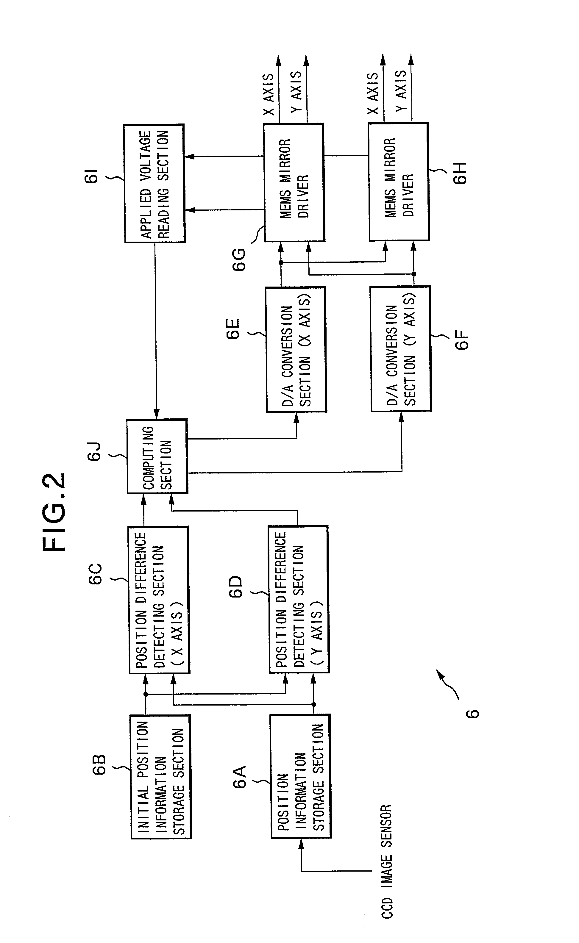
[0070]In FIG. 1, the whole constitution of the first embodiment is such that there is provided a controlling apparatus comprising: a beam splitter 3 as an optical branching section; a lens array 4; a CCD image sensor 5 as a position information generating section; and a control circuit 6 as angle controlling means, concerning a three-dimension type optical switching device constituted by combining two collimator arrays 1A, 1B each having a plurality of collimators two-dimensionally arranged and two MEMS mirror arrays 2A, 2B each having a plurality of MEMS mirrors two-dimensionally arranged so as to correspond to the plurality of collimators, similarly to the conventional constitution shown in FIG. 45. Herein, the MEMS mirror array 2A corresponds to a first mirror array and the MEMS mirror array 2B corresponds to a second mirror a...
second embodiment
[0103]There will be described hereinafter a controlling apparatus of an optical switching device according to the present invention.
[0104]FIG. 13 is a schematic view showing a constitution of an essential part of the controlling apparatus of the optical switching device according to the second embodiment. Like reference numerals as used in the first embodiment are used to denote identical elements in the second embodiment, and the same rule applies corresponding to the following.
[0105]In FIG. 13, the second embodiment is constituted such that a beam splitter 3′ is additionally disposed between the beam splitter 3 and collimator array 1B to the constitution in the aforementioned first embodiment. Light branched by the beam splitter 3′ is received by a CCD image sensor 5′ via a lens array 4′ to generate another position information concerning each optical signal reflected by the MEMS mirror arrays 2A, 2B. Note, the additionally provided beam splitter 3′, lens array 4′ and CCD image se...
third embodiment
[0118]There will be described hereinafter a controlling apparatus of an optical switching device according to the present invention.
[0119]In the aforementioned first and second embodiments, there have been described cases where the angle correction of each MEMS mirror array is performed based on the position information of the optical signal detected by using the CCD image sensor. Differently from these cases, there will be described in the third embodiment such a case where the power of optical signal coupled to the output fiber is monitored, to thereby perform the angle correction of each MEMS mirror based on the monitoring result.
[0120]FIG. 18 is a schematic view showing a whole constitution of the controlling apparatus of the optical switching device according to the third embodiment of the present invention.
[0121]Similarly to the conventional constitution shown in FIG. 45, in the whole constitution of the third embodiment in FIG. 18, there is provided a controlling apparatus co...
PUM
 Abstract
Description
Claims
Application Information


