Semiconductor device

a semiconductor and device technology, applied in the field of semiconductor devices, can solve the problems of insufficient use of digital image data with 8-bit width as high-quality image data, difficult to secure the dynamic range, etc., and achieve the effects of reducing power consumption, simple circuit, and reducing noise sources

Active Publication Date: 2006-10-17
ADVANCED INTERCONNECT SYST LTD
View PDF6 Cites 5 Cited by
  • Summary
  • Abstract
  • Description
  • Claims
  • Application Information

AI Technical Summary

Benefits of technology

[0017]With the semiconductor device in accordance with the present invention, the area sensor and an A / D converter can be formed on the same semiconductor chip, the power consumption can be reduced, analog image signals to digital image data can be converted with a simple circuit, noise sources can be reduced, the cost can be reduce, and the bit width of the digital image data can be compressed while achieving a high dynamic range.

Problems solved by technology

Also, a semiconductor device manufacturing process for CCDs and a semiconductor device manufacturing process for pipeline type A / D converters are completely different from each other, and therefore there is a problem in that the CCDs and pipeline type A / D converter cannot be formed on a single semiconductor chip.
However, the digital image data with 8-bit width is not sufficient in actual use as high-quality image data, and about 10-bit width is normally required.
However, the column type A / D converter has a problem in that it is difficult to secure the dynamic range.
Also, the column type A / D converter has a problem in that the A / D conversion takes a long time because the cycle of the sweep signal in a ramp shape must be made longer in order to achieve a highly accurate A / D conversion.

Method used


Image

  • Semiconductor device
  • Semiconductor device
  • Semiconductor device

Examples


Embodiment Construction

[0027]An embodiment of the present invention is described below with reference to the accompanying drawings. It is noted that the same components are indicated with the same reference numbers, and their description is not repeated.

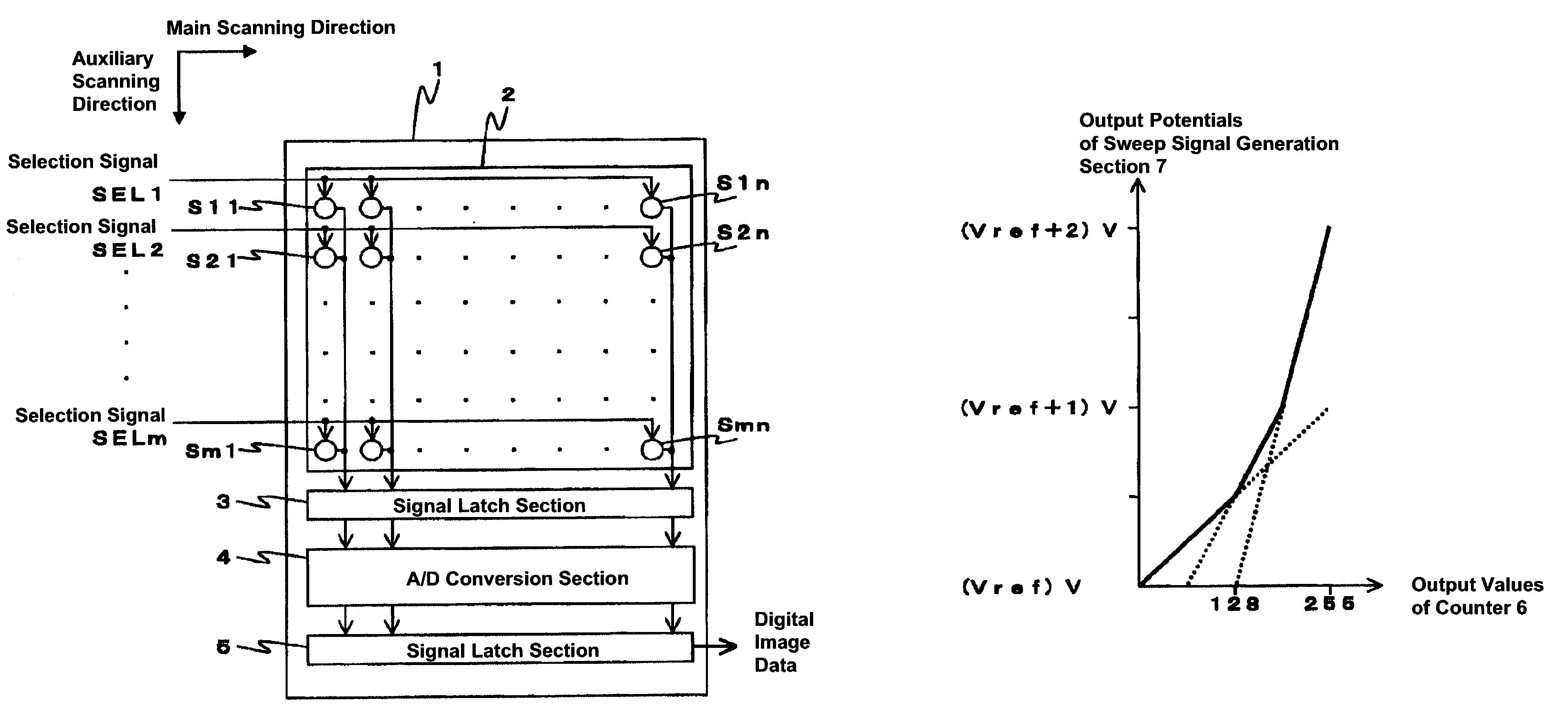
[0028]FIG. 1 shows an outline of a semiconductor device in accordance with an embodiment of the present invention. FIG. 1 shows a semiconductor device 1, which is equipped with an area sensor 2 that outputs analog image signals, a signal latch section 3 that latches the analog image signals output from the area sensor 2, an A / D conversion section 4 that converts the analog image signals output from the signal latch section 3 to digital image data, and a signal latch section 5 that latches and outputs the digital image data output from the A / D conversion section 4.

[0029]The area sensor 2 includes m×n image sensors S11–Smn disposed in a matrix of m rows in the auxiliary scanning direction (common direction) and n columns in the main scanning direction (segme...


PUM


Abstract

A semiconductor device equipped with an area sensor 2 including a plurality of image sensors S11–Smn outputting analog image signals corresponding to the amount of received light; an A / D conversion section 4 including a signal latch section 3 latching the analog image signals, a counter 6 that successively increments integer values and outputs the same, a sweep signal generation section 7 outputting sweep signals whose potential rises in a polygonal line with respect to the integer values, comparators C1–Cn comparing the analog image signals and the sweep signals, and outputting high level signals when the sweep signals are greater than the analog image signals, and latches L1–Ln latching and outputting integer values when signals output from the comparators C1–Cn become a high level; and a signal latch section 5 latching digital image data output from the A / D conversion section 4 and outputting the same.

Description

BACKGROUND OF THE INVENTION[0001]1. Technical Field of the Invention[0002]The present invention relates to a semiconductor device that photographs images and outputs digital image data.[0003]2. Prior Art[0004]In recent years, digital still cameras and digital video cameras with over one million pixels have come into use. These digital still cameras and the like are quipped with an area sensor and an A / D converter, and obtain digital image data by digitally converting output signals (analog image signals) of the area sensor by the A / D converter. Digital still cameras and the like used in recent years need an A / D conversion speed of about 20 MHz–30 MHz, and therefore often use pipeline type A / D converters that are capable of performing high-speed A / D conversion. FIG. 6 shows an example of a conventional circuit (digital image photographing circuit) for photographing digital images. Referring to FIG. 6, the digital image photographing circuit 40 is equipped with an area sensor 41 havin...

Claims


Application Information

Patent Timeline
Patent Type & Authority Patents(United States)
IPC IPC(8): H04N3/14H03M1/08H03M1/18H03M1/48H04N5/335H04N5/355H04N5/374H04N5/378
CPCH04N3/155H04N5/335H04N25/75
Inventor SHIOHARA, RYUICHI
Owner ADVANCED INTERCONNECT SYST LTD
Why Eureka
Try Eureka