Phase change memory and phase change recording medium

a technology of phase change and recording medium, which is applied in the field of phase change memory or phase change recording medium, can solve the problems of difficult distinction from the amorphous phase, the irregularity of the crystalline state, and the difficulty of the erased state, and achieve the effect of high reliability

Inactive Publication Date: 2006-10-24
RENESAS TECH CORP
View PDF8 Cites 166 Cited by
  • Summary
  • Abstract
  • Description
  • Claims
  • Application Information

AI Technical Summary

Benefits of technology

[0004]A first object of the present invention is to provide a phase change memory and a recording medium with high reliability.
[0005]A second object of the present invention is to provide a phase change memory and a recording medium, which preserves its excellent performance even after repetition of writing and reading.
[0009]Concretely, for example, it is possible to provide a phase change memory or recording medium with high reliability.
[0010]Alternatively, further, it is possible to provide a phase change memory and a phase change recording medium with high rewriting repetition tolerance.

Problems solved by technology

Further, with respect to the above teaching in “Applied Physics”, the inventors have found that if a composition with high density of lattice imperfection is employed to improve repetition tolerance, regularity of an atomic arrangement in the crystalline state (i.e. erased condition) becomes inferior as an adverse effect due to increase of lattice imperfection and distinction from the amorphous phase becomes difficult.

Method used


Image

  • Phase change memory and phase change recording medium
  • Phase change memory and phase change recording medium
  • Phase change memory and phase change recording medium

Examples


first embodiment

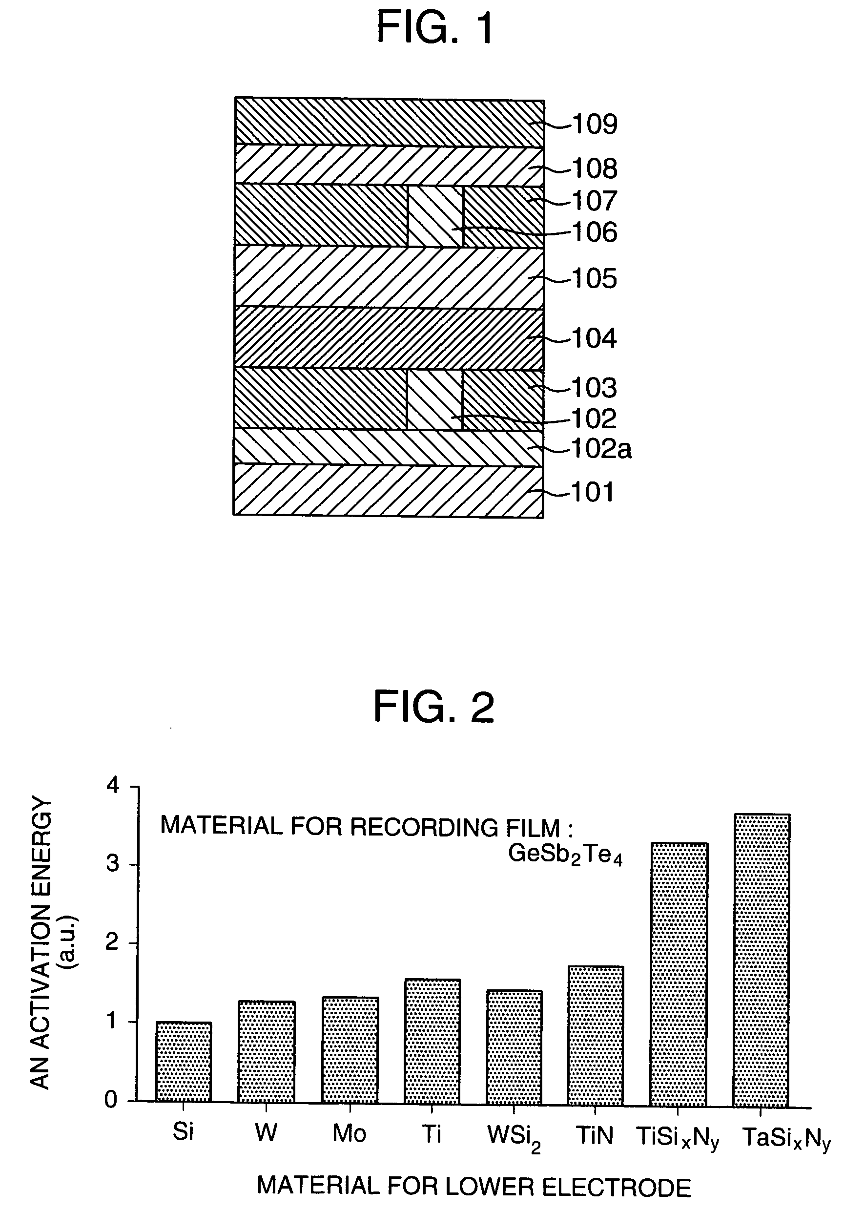
[0042]FIG. 1 shows a sectional structure of a main part of a phase change memory according to the present invention. A general outline of a phase change memory is described in Applied Physics Vol. 71, No. 12 (2002), pp. 1513–1217. A phase change memory of the embodiment of the present invention is fabricated by successively overlaying a wiring film 102a, a lower electrode film 102, an insulation film 103, a phase change recording film 104, an upper electrode film 105, a wiring film 106, an insulation film 107, a wiring film 108 and then an insulation film 109 on a silicon substrate 101, for example. Each films may be formed by sputtering, CVD, plating or else.

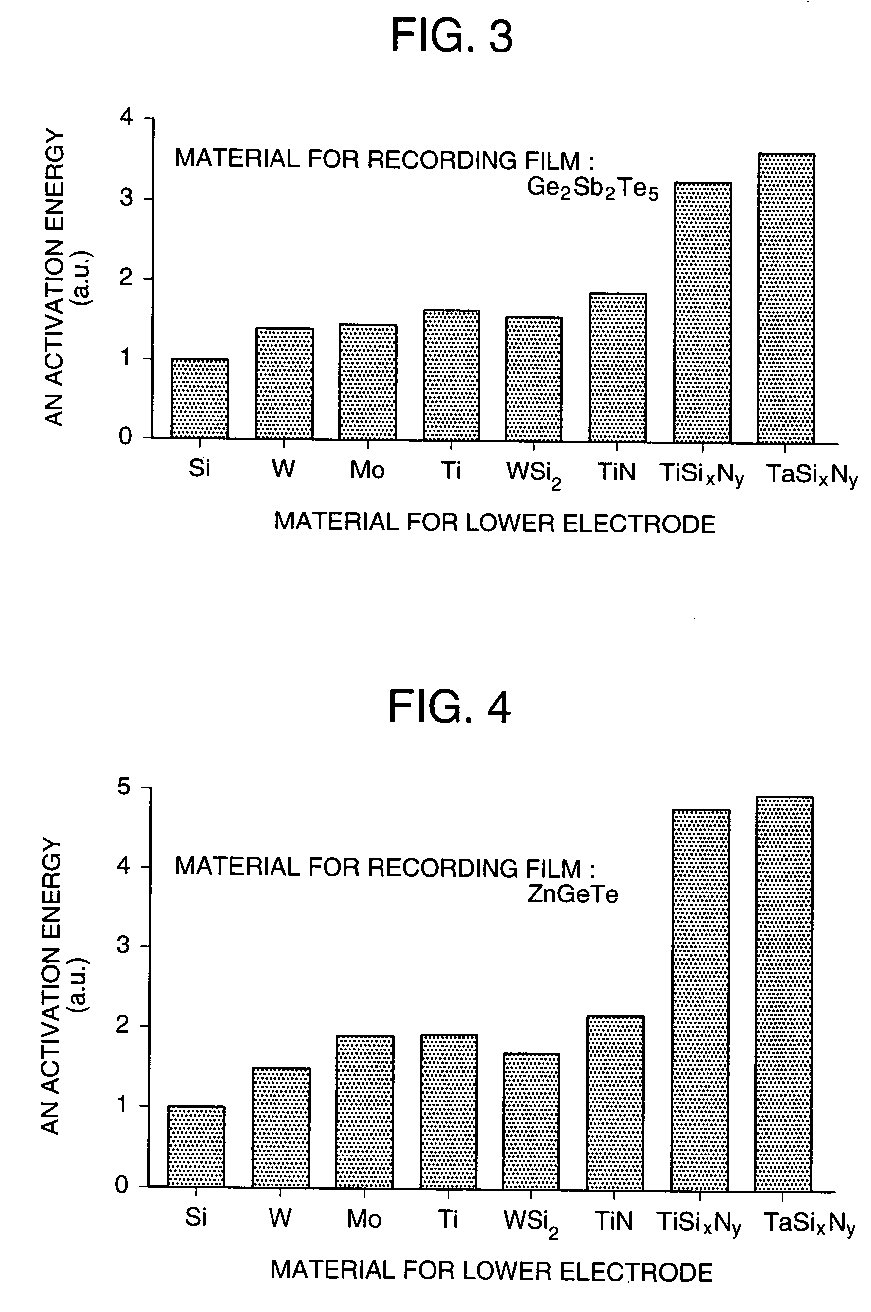
[0043]The phase change recording film 104 preferably contains at least two constituting elements selected from Ge, Sb and Te. It is preferable to contain Te. For example, GeSb2Te4, Ge2Sb2Te5, Ge6Sb2Te9, ZnSbxTey, ZnGexTey, ZnGexSbyTez or GeSbxTey may be a main constituting material. GeSb2Te4, Ge2Sb2Te5 and Ge6Sb2Te9 have an adv...

fifth embodiment

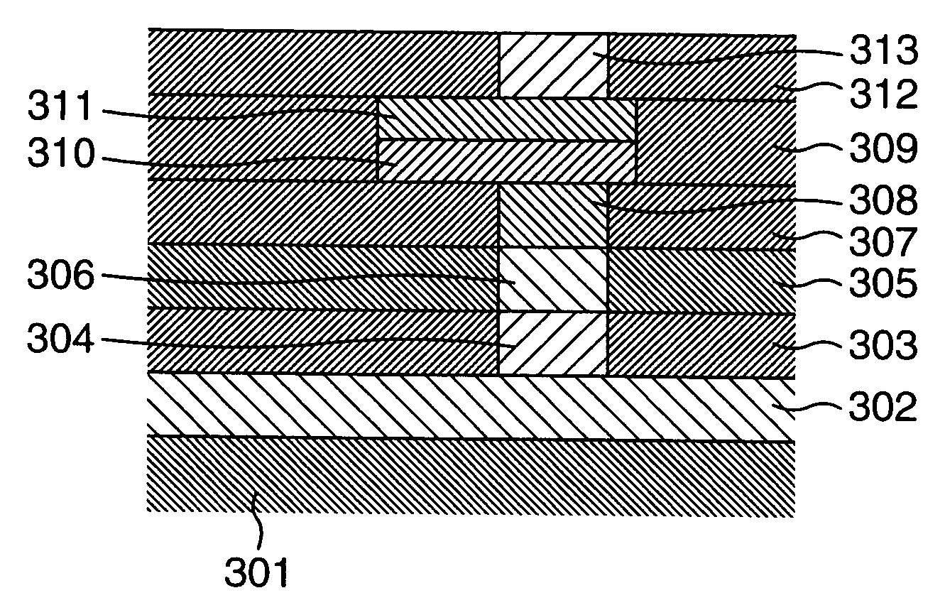
[0072]FIG. 12 schematically illustrates a sectional structure of a main portion of a phase change memory of the present invention. In the present phase change memory, a gate insulation film 202 and a gate electrode 206, which structure a transistor, are formed on a silicon substrate 201, for example, and further wiring is formed in diffusion layers 203 and 204 as source and drain.

[0073]The phase change memory in FIG. 12 has wiring 208a in electrically communication with the diffusion layer 204, wiring 208b in electrically communication with the diffusion layer 203, and wiring 215, 217, 219. A lower electrode film 210 in electrically communication with the wiring 208b, a phase change recording film 212 deposited on the lower electrode film 210, and an upper electrode film 213 deposited on the phase change recording film 212, are isolated by insulation layers 207, 209, 211, 214, 216 and 218.

[0074]A transistor, which is composed of the gate electrode 206, the gate insulation film 202 a...


PUM

PropertyMeasurementUnit
average distanceaaaaaaaaaa
phase change memoryaaaaaaaaaa
concentrationaaaaaaaaaa

Abstract

A phase change memory comprises: a substrate; an insulation film formed on a main surface of the substrate; a first electrode deposited on the insulation film; a phase change recording film deposited on the first electrode; and a second electrode deposited on the phase change recording film. The phase change recording film contains at least two of Ge, Sb and Te as main constituting elements thereof. The first electrode comprises material of group of Ti, Si and N, or group of Ta, Si and N as main constituting material thereof.

Description

BACKGROUND OF THE INVENTION[0001]The present invention relates to a phase change memory or a phase change recording medium, which is capable of recording / reproducing information by utilizing phase change.[0002]In phase change recording method, recording is performed by unitizing a fact that material for a recording film undergoes phase change between crystal phase and amorphous phase and reading is performed by judging whether the recording film material is in the crystal phase or the amorphous phase, as disclosed in Applied Physics Vol. 71, No. 5 (2002) pp. 562–565, for example.[0003]A chalcogenide, e.g. GeSbxTey, is representative recording film material in such phase change recording method, but its amorphous phase is unstable and sometimes crystallized with the lapse of time. This trouble becomes worse under circumstances of high temperature. Further, there is a problem that properties of the recording film material are degraded by repetition of rewriting in a case where volume ...

Claims


Application Information

Patent Timeline
Patent Type & Authority Patents(United States)
IPC IPC(8): H01L47/00H01L29/04B41M5/26G11B7/24G11B7/2403G11B7/24033G11B7/241G11B7/243G11B7/2433G11B7/2437G11B7/252G11B7/254G11B7/257H01L27/24H01L29/02H01L45/00
CPCG11B7/2403G11B7/243G11B7/252G11B7/257G11C13/0004H01L45/1253H01L45/06H01L45/1233H01L45/144G11B7/00454G11C2213/72G11C2213/79H01L27/2409H01L27/2436H10B63/20H10B63/30H10N70/841H10N70/231H10N70/8828H10N70/826
Inventor IWASAKI, TOMIOMORIYA, HIROSHIMATSUOKA, HIDEYUKITAKAURA, NORIKATSU
Owner RENESAS TECH CORP
Why Eureka
Try Eureka