

Interlocking memory/logic cell layout and method of manufacture
- Summary
- Abstract
- Description
- Claims
- Application Information
AI Technical Summary
Benefits of technology
Problems solved by technology
Method used
Image

Examples
Embodiment Construction
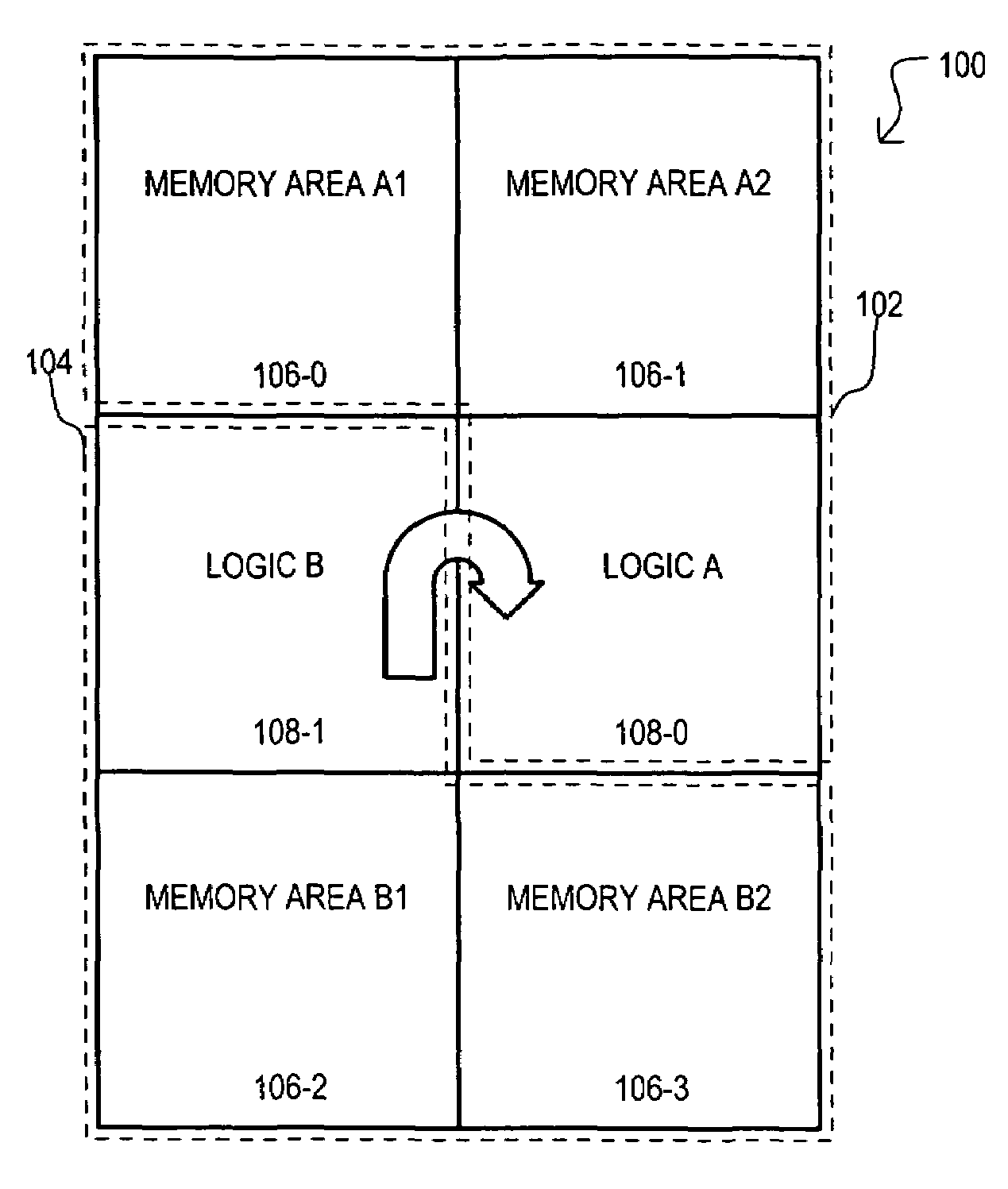
[0039]The present invention is directed to a novel layout for a circuit that employs memory circuits in conjunction with corresponding logic circuits, including but not limited to programmable logic (PLD) circuits and / or content addressable memory (CAM) devices, including both ternary CAM (TCAM) devices, “pseudo” TCAM devices, and binary CAM devices. The disclosed layouts can include a pair of memory / logic cells that can occupy less area on a die or substrate on which they are formed over conventional approaches.
[0040]A layout structure according to one embodiment of the present invention will now be described with reference to FIG. 1. For purposes of clarity, many of the details of particular memory / logic cells and the methods of designing and manufacturing the same that are widely known and are not relevant to the present invention have been omitted from the following description.
[0041]FIG. 1 is a block diagram of a pair of interlocking memory / logic cells showing an embodiment of ...
PUM
 Abstract
Description
Claims
Application Information