Methods of manufacture for a low control voltage switch
a manufacturing method and low control voltage technology, applied in the field of switch devices, can solve the problems of poor isolation of switch, increased cost of switch, and increased manufacturing cost of semiconductor materials
- Summary
- Abstract
- Description
- Claims
- Application Information
AI Technical Summary
Benefits of technology
Problems solved by technology
Method used
Image
Examples
Embodiment Construction
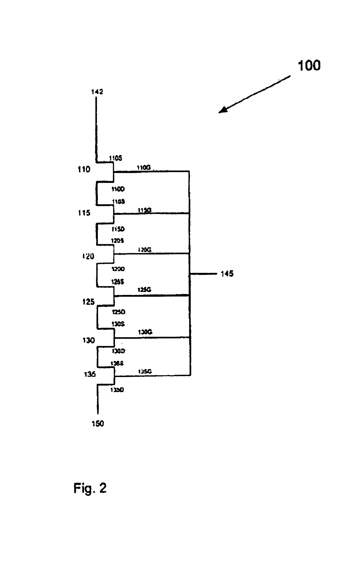
[0039]FIG. 2 illustrates an exemplary schematic diagram of one embodiment of a switch 100 of the present invention. As illustrated, the switch 100 includes six field effect transistors (FETs) 110, 115, 120, 125, 130, and 135 connected together in series. Each FET has a source 110S-135S, a gate 110G-135G, and a drain 110D-135D. The drain of one FET is connected to the source of the next FET (i.e., drain 110D is connected to source 115S). The source 110S of the first FET 110 is connected to a source voltage input 142 that provides a source voltage for the switch 100. Each of the gates 110G-135G is coupled together and connected to a control voltage input 145 that provides a control voltage. The drain 135D of the sixth FET 135 is connected to an output 150 that will provide the current to a load. The use of six FETs, having six gates, allows the switch 100 operate at a low control voltage without the need to increase device periphery or die size.
[0040]The switch 100 is not limited to s...
PUM
 Abstract
Description
Claims
Application Information


