Electronic device and method of driving electronic device

a technology of electronic devices and electronic devices, applied in closed circuit television systems, instruments, television systems, etc., can solve the problems of reduced duty ratio and insufficient brightness, and achieve the effect of reducing duty ratio, increasing duty ratio, and sufficient sustain (turn-on) periods

Inactive Publication Date: 2006-10-31
SEMICON ENERGY LAB CO LTD
View PDF9 Cites 88 Cited by
  • Summary
  • Abstract
  • Description
  • Claims
  • Application Information

AI Technical Summary

Benefits of technology

[0041]The main cause of insufficient brightness is a reduced duty ratio in accordance with the above stated problem points. The present invention is created in view of these types of problems, and an object of the present invention is to ...

Problems solved by technology

The main cause of insufficient brightness is a reduced ...

Method used


Image

  • Electronic device and method of driving electronic device
  • Electronic device and method of driving electronic device
  • Electronic device and method of driving electronic device

Examples


embodiment 1

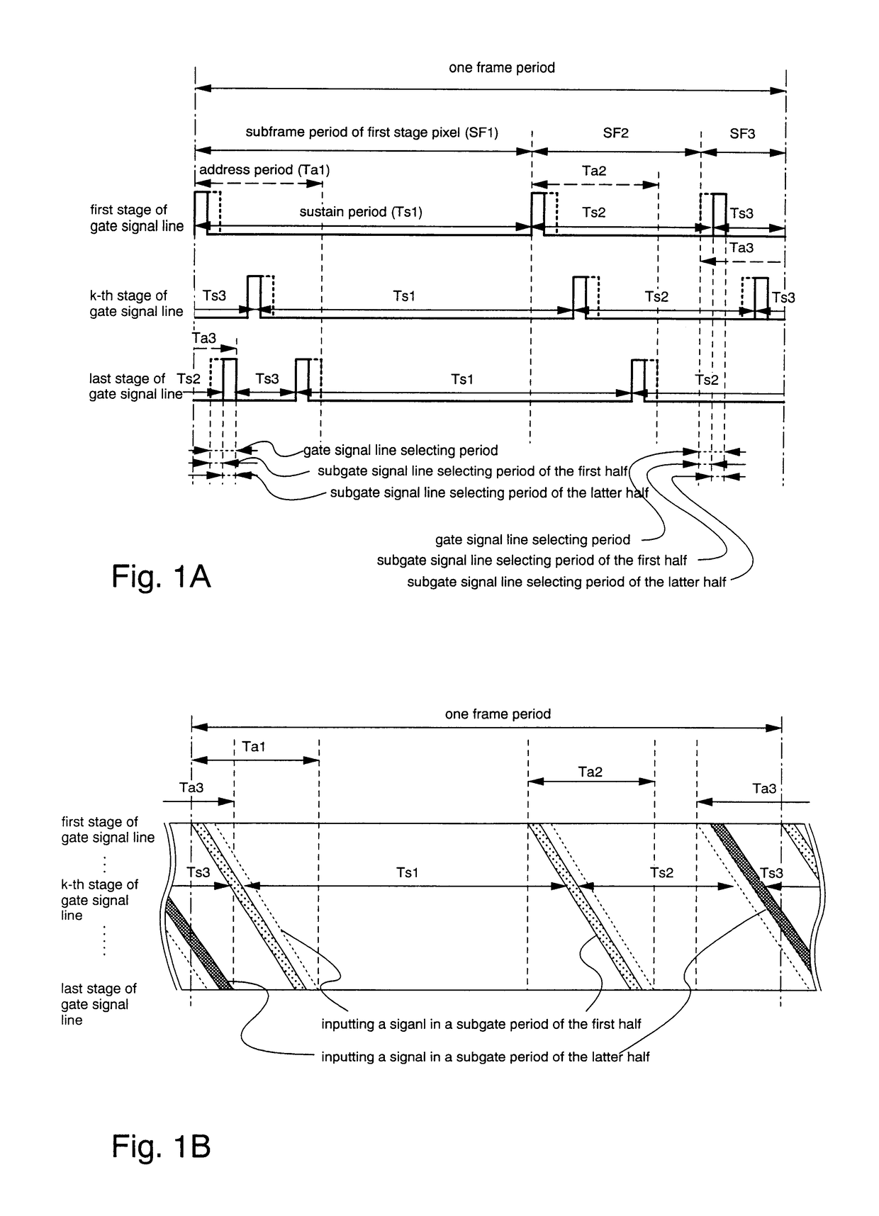
[0174]A case in which there are a plurality of subframe periods having sustain (turn on) periods which are shorter than address (write in) periods when dividing one frame period is given as an example and explained in Embodiment 1.

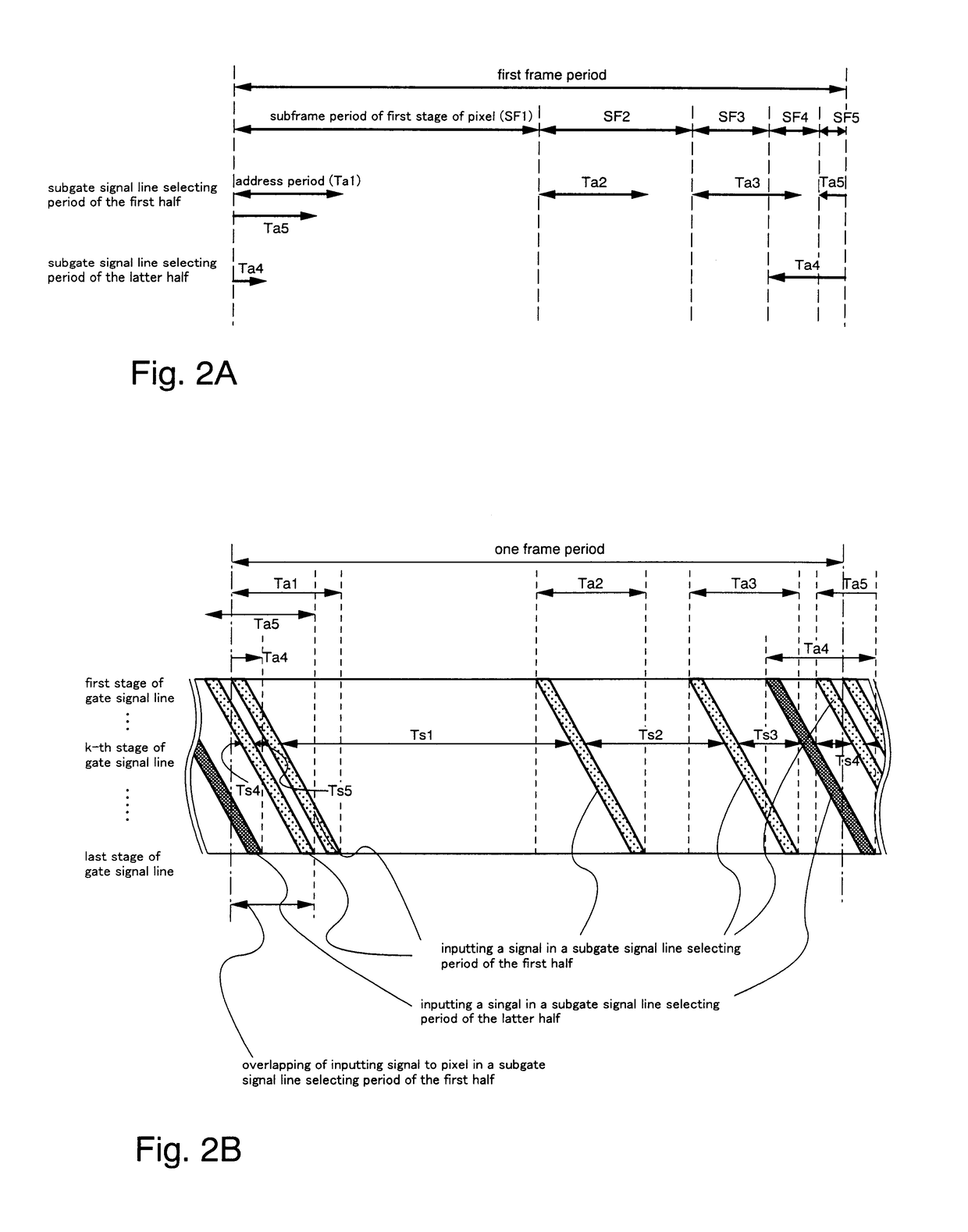
[0175]FIGS. 2A and 2B are referred to. FIGS. 2A and 2B show timing charts when dividing one frame period into five subframe periods. In this case, it can be seen that even if the gate signal line selection period is divided into the first half and the second half sub-gate signal line selection periods, and write in of a signal is performed, an address (write in) period Ta5 and an address (write in) period Ta1 of the next frame period will overlap. Normal signal write in therefore cannot be performed at this timing.

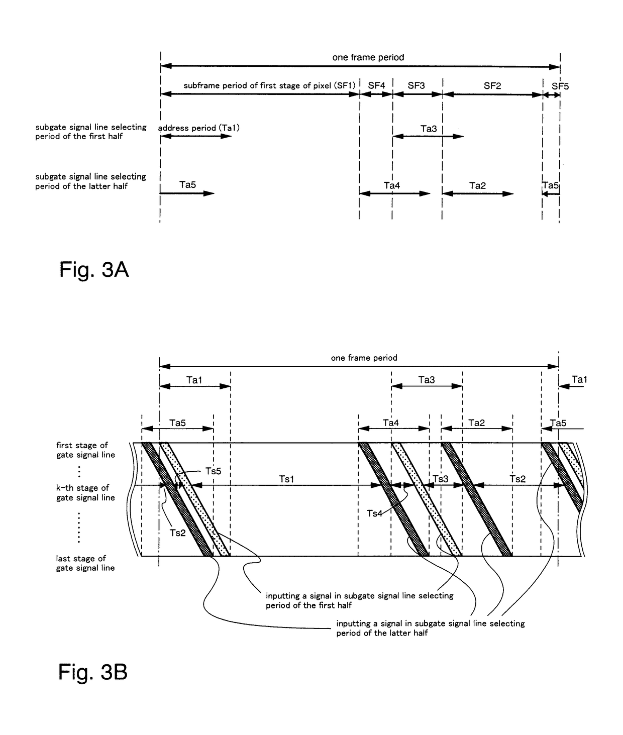
[0176]This problem can be resolved in accordance with interchanging the order of long subframe periods and short subframe periods, as one method. FIGS. 3A and 3B are referenced. FIGS. 3A and 3B show timing charts when dividing one frame period in...

embodiment 2

[0177]A method of avoiding overlap of address (write in) periods by a means which differs from that of Embodiment 1 is explained in Embodiment 2.

[0178]In FIGS. 2A and 2B, the address (write in) periods which overlap are Ta5 and Ta1 of the next frame period. This problem can be resolved by dividing the gate signal line selection periods into three sub-gate signal line selection periods and partitioning the write in of a signal into a first, a second, and a third sub-gate signal line selection period. FIGS. 4A and 4B are referred to. Signal write in is performed in Ta1, Ta2, and Ta3 in the first sub-gate signal line selection period, signal write in is performed in Ta4 in the second sub-gate signal line selection period, and signal write in is performed in Ta5 in the third sub-gate signal line selection period. As a result, signal write in is performed at a timing like that shown in FIG. 4B, and overlap of a plurality of address (write in) periods within each sub-gate signal line sele...

embodiment 3

[0180]A method of avoiding overlap of address (write in) periods by a means which differs from that of Embodiment 1 and Embodiment 2 is explained in Embodiment 3.

[0181]FIGS. 5A and 5B are referred to. The period of SF4 and SF5 themselves is short, and overlap of address (write in) periods cannot be avoided at a normal timing. Reset periods Tr4 and Tr5 are therefore formed after SF4 and SF5, respectively. A signal is input during the reset periods such that the OLED elements do not turn on. Specifically, the write in voltage may be a voltage in which electric charge does not accumulate in the storage capacitor. This signal is hereafter referred to as a reset signal. By changing the period from when the signal is written into the pixels until the reset signal is input, the lengths of the subframe periods SF4 and SF5 can be regulated, and the timing may be set such that each address (write in) period and reset period do not overlap.

[0182]A problem develops in that the OLED elements do ...


PUM


Abstract

Problems such as insufficient brightness, caused by a reduction in duty ratio (the ratio of a light emitting period and a non-light emitting period), are improved upon in accordance with using a novel method of driving and a novel circuit in an electronic device. Signals are written into pixels of a plurality of differing lines during one gate signal line selection period. By arbitrarily setting, to a certain extent, the time from when a signal is input into the pixels of a certain line until the next signal is input to the same pixels, while ensuring the time for writing into the pixels, a sustain (turn on) period can be arbitrarily set and a high duty ratio is realized.

Description

BACKGROUND OF THE INVENTION[0001]1. Field of the Invention[0002]The present invention relates to an electronic device and to a method of driving an electronic device. In particular, the present invention relates to an active matrix electronic device having a thin film transistor (TFT) formed on an insulating substrate, and to a method of driving an active matrix electronic device. From among all active matrix electronic devices, the present invention relates, in particular, to an active matrix electronic device using a self light emitting element, such as an OLED (Organic Light Emitting Diode) element, and to a method of driving such an active matrix electronic device.[0003]2. Description of the Related Art[0004]OLED displays have been gathering attention in recent years as flat display substitutes for LCDs (liquid crystal displays), and research into OLED displays is proceeding apace.[0005]LCDs can roughly be divided into two types of driving methods. One is a passive matrix type u...

Claims


Application Information

Patent Timeline
IPC IPC(8): G09G3/30G09G3/20G09G3/32
CPCG09G3/3266G09G3/3275G09G3/2018G09G3/2022G09G2300/0426G09G2300/0814G09G2300/0842G09G2300/0861G09G2310/0205G09G2310/0251G09G2310/027G09G2320/0233
Inventor KIMURA, HAJIME
Owner SEMICON ENERGY LAB CO LTD
Why Eureka
Try Eureka