Telecommunication line driver having synthesized output impedance derived from output current sensing circuit

Inactive Publication Date: 2006-10-31
ADTRAN
View PDF4 Cites 5 Cited by
  • Summary
  • Abstract
  • Description
  • Claims
  • Application Information

AI Technical Summary

Benefits of technology

[0016]A second auxiliary current mirror circuit is coupled to the current mirror circuit and to the inverting input of the operational amplifier to which a second auxiliary bias current source is coupled. Coupling the second auxiliary bias current source to the inverting input of the operational amplifier effec

Problems solved by technology

Prior to the introduction of synthetic drivers, this meant not matching the driver's output impedance to that of the line.
However, as customers of telecommunication equipment have become less careful about controlling the impedance of DSX-1 cross-connect cables in central office installations,

Method used


Image

  • Telecommunication line driver having synthesized output impedance derived from output current sensing circuit
  • Telecommunication line driver having synthesized output impedance derived from output current sensing circuit
  • Telecommunication line driver having synthesized output impedance derived from output current sensing circuit

Examples


first embodiment

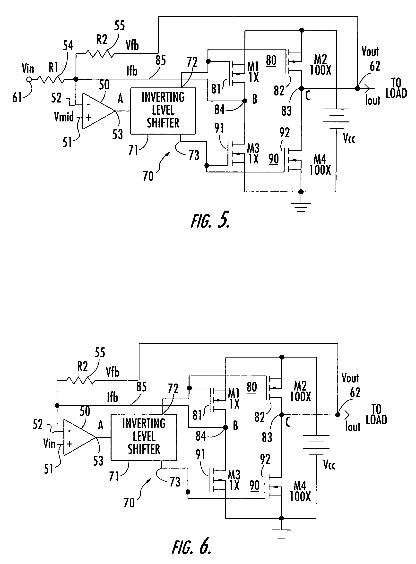
[0034]As referenced above, FIG. 5 shows a single ended implementation of the sensed output current-based synthesized impedance line driver of the invention. To compensate for distortion that may result from non-linearities in the ratios of the geometries of the current mirror and output MOSFETs a pair of the drivers of FIG. 5 may be coupled in a bridge configuration.

[0035]The fact that output MOSFETs 82, 92 and current mirror MOSFETs 81, 91 of FIG. 5 do not see the same drain-source voltage can be a significant source of distortion, preventing the mirror current MOSFETs 81 and 91 from tracking output MOSFETs 82 and 92, respectively. This problem is remedied by the embodiment of FIG. 6, in which the input resistor 54 of FIG. 5 is removed, and the input Vin is applied to the non-inverting (+) input 51 of operational amplifier 50. Due to the high gain of the amplifier 50, both of its inputs 51 and 52 are maintained at substantially the same voltage.

[0036]In the no-load case, the voltag...

third embodiment

[0037]As shown in FIG. 7, this effect can be compensated for a given load impedance by inserting a first auxiliary resistor 86 (having a value R4) in the mirrored current feedback path 85, and coupling the current mirror node 84 through a second auxiliary resistor 87 (having a value R3) to the reference voltage (Vmid) applied to the non-inverting input 51 of amplifier 50. Defining the mirrored current ratio Ifb / Iout as k, the output impedance Zout of the embodiment of FIG. 7 becomes

Zout={(k*R2*R3) / (R3+R4)}*{1+(k*R3) / (R3+R4)}.

[0038]If V84 is constrained to equal V83 for a given value of load resistance RL, then (k*R3*R4) / (R3+R4)=RL||R2.

[0039]By choosing k and Vout as independent variables, the values of R2, R3 and R4 are to be determined. It may be noted that R1 is only a portion of the open circuit voltage expression: Vout / Vin={−R2 / R1}*{1 / (1+(k*R3) / (R3+R4)}. As a result, there are the impedance constraining equation (Zout=RL), the voltage matching equation, and three unknowns. Altho...

fourth embodiment

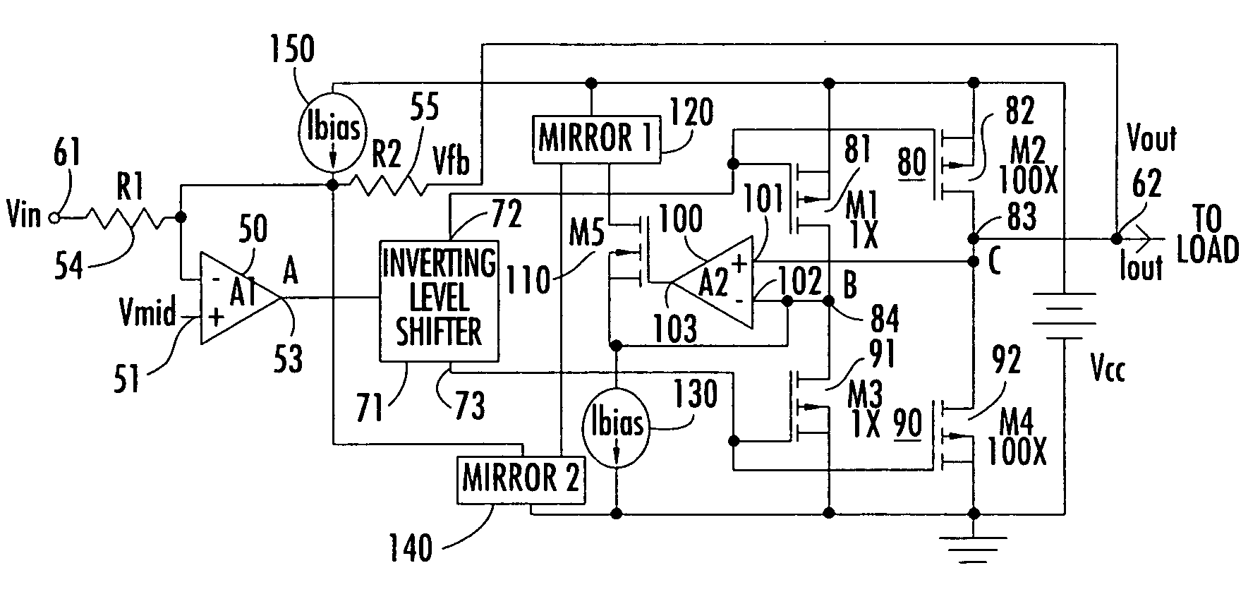
[0045]FIG. 8 shows the invention, which is configured to ensure that the voltage at the current mirror node 84 always tracks the output voltage at the output current node 83, and thereby removes current mirror distortion for all values of load resistance. For this purpose, a second, ‘feedback’ operational amplifier 100 has a first, non-inverting (+) input 101 coupled to node 83 and a second inverting (1) input 102 coupled to the current mirror node 84. The output 103 of the feedback operational amplifier 100 is coupled as the gate drive for a MOSFET 110, which has its source-drain path coupled to voltage rails Vcc and GND through a first auxiliary current mirror circuit 120 and a first auxiliary bias current (Ibias) source 130, referenced to GND, respectively. The first auxiliary bias current (Ibias) source 130 serves to maintain MOSFET 110 conducting for both polarities of output current (and also current through MOSFETs 81, 91).

[0046]A second auxiliary current mirror circuit 140 i...


PUM


Abstract

A synthetic impedance telecommunication line driver has no electrical energy-dissipating elements in series with its output, and synthesizes its output impedance in accordance with current fed back from an output current (mirror) sensing circuit. This allows the driver to realize substantially reduced power requirements for driving a telecommunication line, such as, but not limited to a DSX-1 line. The driver includes an operational amplifier having a first polarity input coupled through an input resistor to an input port, to which a signal voltage to applied to an output port is coupled. A second polarity input of the amplifier is coupled to a reference voltage. A feedback resistor is coupled between the amplifier output and its inverting input. An output current-dependent current source, such as a current mirror coupled in circuit with the output node, generates a current as a small fraction k of the output current. This mirrored fraction of the output current is fed back to an input of the amplifier, and enables the output impedance Zout of the driver to be defined in terms of the mirror current ratio k and the value of the driver amplifier's feedback resistor.

Description

FIELD OF THE INVENTION[0001]The present invention relates in general to communication systems and components, and is particularly directed to a synthetic impedance telecommunication line driver, that has no electrical energy-dissipating elements in series with its output, and synthesizes its output impedance in accordance with current fed back from an output current (mirror) sensing circuit, so as to realize substantially reduced power requirements for driving a communication line, such as a DSX-1 line.BACKGROUND OF THE INVENTION[0002]For optimum efficiency, a telecommunication line driver should contain no dissipative elements in series with its output. Prior to the introduction of synthetic drivers, this meant not matching the driver's output impedance to that of the line. Until recently, this has not been a problem in a T1 DSX environment, as the terminating end was well matched to the line impedance, and the line impedance was homogeneous as a result of strict control of the typ...

Claims


Application Information

Patent Timeline
IPC IPC(8): H04M19/00H04M1/76
CPCH04M1/76H04M19/005Y02D30/70
Inventor JOFFE, DANIEL M.GEWIN, ROBERT E.FORAN, CHRISTOPHER J.
Owner ADTRAN
Why Eureka
Try Eureka