Back-lit image sensor

a back-lit image sensor and image sensor technology, applied in the field of image sensors, can solve the problems of disturbance of the signals read from the read nodes of the photosensitive cells, difficulty in formation, and difficulty in forming image sensors, so as to reduce or even eliminate the disturbance of dark currents

Inactive Publication Date: 2008-01-03
STMICROELECTRONICS SRL
View PDF6 Cites 27 Cited by
  • Summary
  • Abstract
  • Description
  • Claims
  • Application Information

AI Technical Summary

Benefits of technology

[0020]A feature of at least one embodiment of the present invention is a back-lit image sensor enabling a decrease, or even elimination of dark current dist

Problems solved by technology

A disadvantage of such a structure is that the straight travel of the light rays from each lens to the associated photodiode may be hindered by the metal tracks and vias present at the level of the stacking of insulating layers covering the substrate.
This results in image sensors that may have a relatively complex structure, and are difficult to form.
In the absence of specific processings, such electrons of thermal origin are likely to be captured by the photodiodes of the image sensor, causing a disturbance of the signals read from the read nodes of the photosensitive cells.
The main disadvantage of previously-described conventional methods for manufacturing image sensors i

Method used


Image

  • Back-lit image sensor
  • Back-lit image sensor
  • Back-lit image sensor

Examples


Embodiment Construction

[0043]For clarity, the same elements have been designated with the same reference numerals in the different drawings and, further, as usual in the representation of integrated circuits, the various drawings are not to scale.

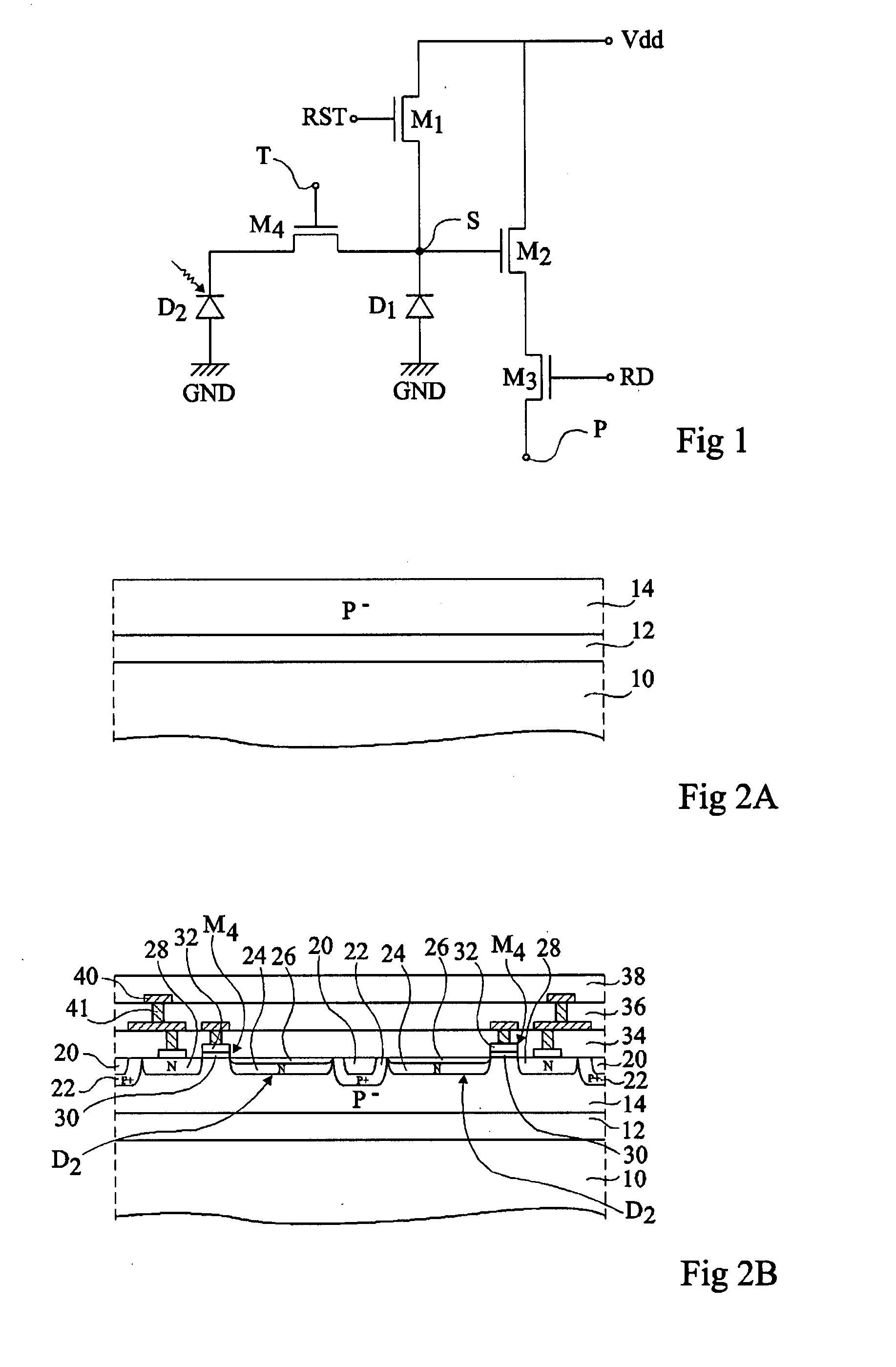
[0044]An example of a method for manufacturing an image sensor or photodetector according to the present invention will now be described. As an example, it is started from a structure of silicon-on-insulator type such as shown in FIG. 2A.

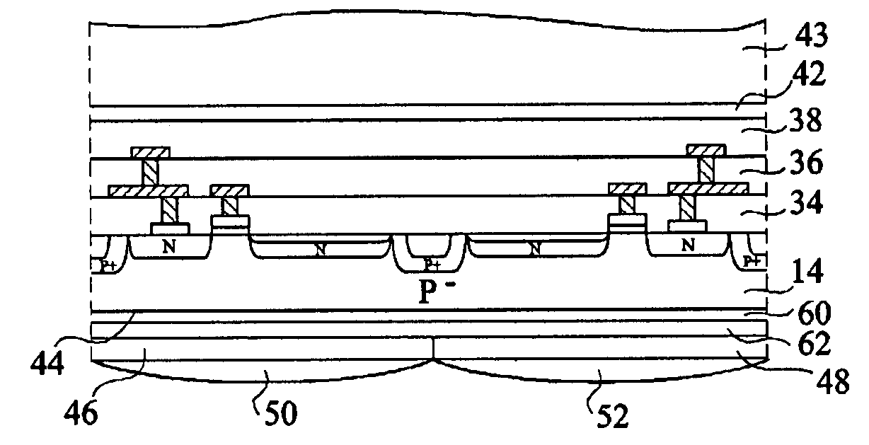
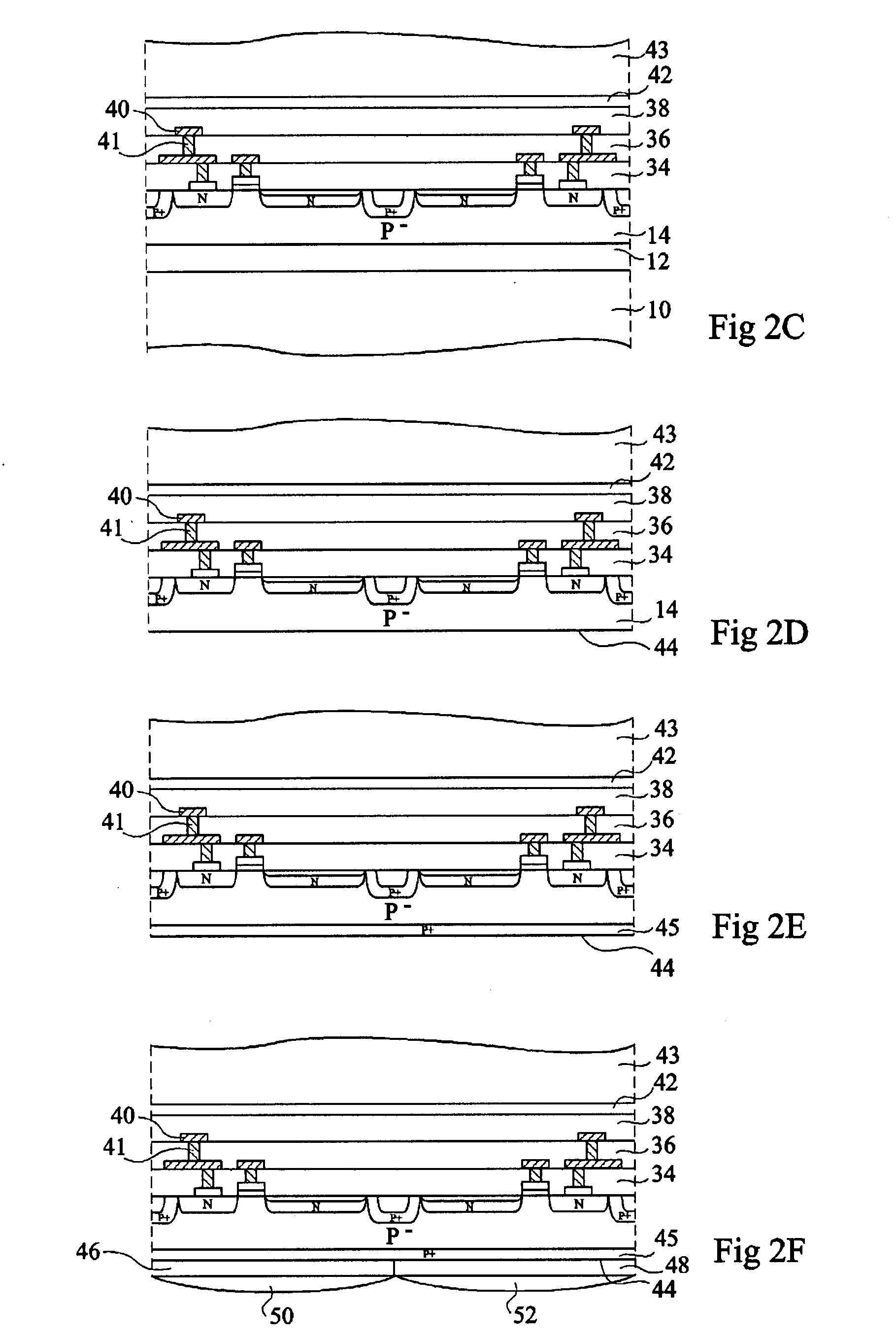
[0045]FIG. 3A is a drawing similar to FIG. 2B and shows the structure obtained after having formed the photosensitive cell components, the stack of insulating layers 34, 36, 38, metal tracks 40, and metal vias 41. The next steps of the example of the method according to the present invention correspond to the steps of the conventional method for manufacturing of an image sensor previously described in relation with FIG. 2C.

[0046]FIGS. 3B and 3C illustrate the last steps of the example of a manufacturing method according to at lea...


PUM


Abstract

An image sensor including a substrate of a semiconductor material having first and second opposite surfaces; at least one photodiode formed in the substrate on the first surface side and intended to be lit through the second surface; a stacking of insulating layers covering the first surface; and conductive regions formed at the stacking level. The sensor further includes a transparent insulating layer at least partly covering the second surface; a transparent conductive layer at least partly covering the transparent insulating layer; and circuitry for biasing the conductive layer.

Description

BACKGROUND OF THE INVENTION[0001]1. Field of the Invention[0002]The present invention relates to an image sensor made in monolithic form capable of being used in shooting devices such as, for example, film cameras, camcorders, digital microscopes, or again digital photographic cameras. More specifically, the present invention relates to a photosensitive cell based on semiconductors.[0003]2. Discussion of the Related Art[0004]FIG. 1 schematically illustrates an example of a circuit of a photosensitive cell of an array of photosensitive cells of an image sensor. With each photosensitive cell of the array is associated a precharge device and a read device. The precharge device is formed of an N-channel MOS transistor M1, interposed between a supply rail Vdd and a read node S. The gate of precharge transistor M1 is capable of receiving a precharge control signal RST. The read device is formed of the series connection of first and second N-channel MOS transistors M2, M3. The drain of fir...

Claims


Application Information

Patent Timeline
IPC IPC(8): H01L31/113H01L31/18
CPCH01L27/1462H01L27/14627H01L27/14643H01L27/1464H01L31/02161H01L31/0232H01L27/14685
Inventor ROY, FRANCOIS
Owner STMICROELECTRONICS SRL
Why Eureka
Try Eureka