Semiconductor device

a technology of semiconductors and devices, applied in the direction of semiconductor devices, basic electric elements, electrical appliances, etc., can solve the problems of increasing device pitch and increasing on-resistance, and achieve the effects of high operation speed, reduced switching losses, and high integration

Inactive Publication Date: 2005-03-24
FUJI ELECTRIC HLDG CO LTD
View PDF5 Cites 27 Cited by
  • Summary
  • Abstract
  • Description
  • Claims
  • Application Information

AI Technical Summary

Benefits of technology

The invention was made in view of the above problems with an object of providing a semiconductor device provided with a trench lateral IGBT (hereinafter referred to as a TL-IGBT) having a small device pitch by which the IGBT can be highly integrated. Moreover, it is also an object of the invention to eliminate the substrate current of the TL-IGBT in a semiconductor device provided with the TL-IGBT, to enable realization of a reduction in switching losses and a high operation speed.

Problems solved by technology

Therefore, integration of the TLPM and a CMOS device for controlling the TLPM has a possibility of causing latchup due to interaction between transistors.
Moreover, there also arises a problem that the laterally extended drift region causes an increase in the device pitch, which in turn results in an increase in on-resistance.

Method used


Image

  • Semiconductor device
  • Semiconductor device
  • Semiconductor device

Examples


Embodiment Construction

In the following, embodiments of the invention will be explained in detail in terms of modes for carrying out the invention, with reference to drawings.

First Mode

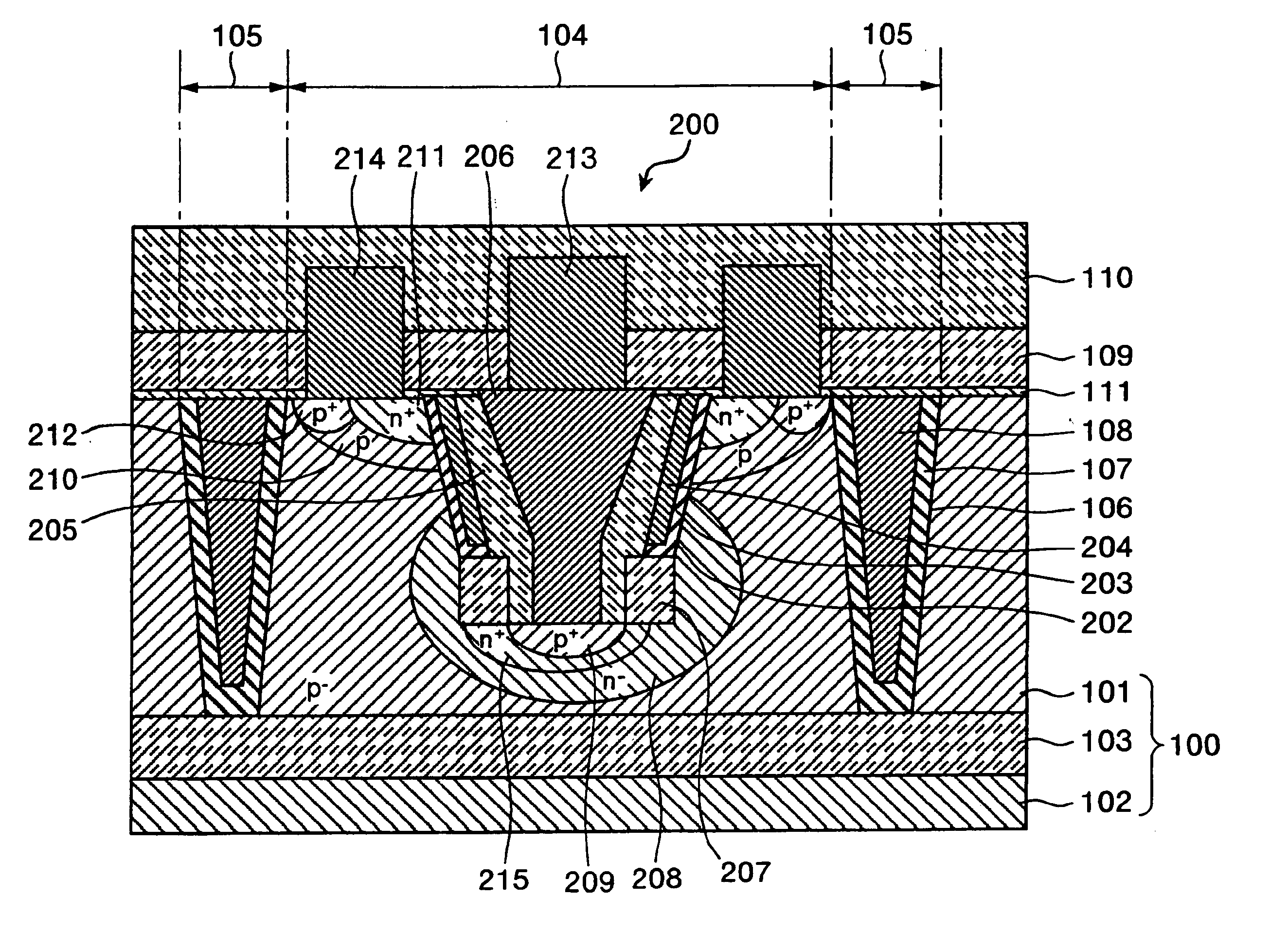
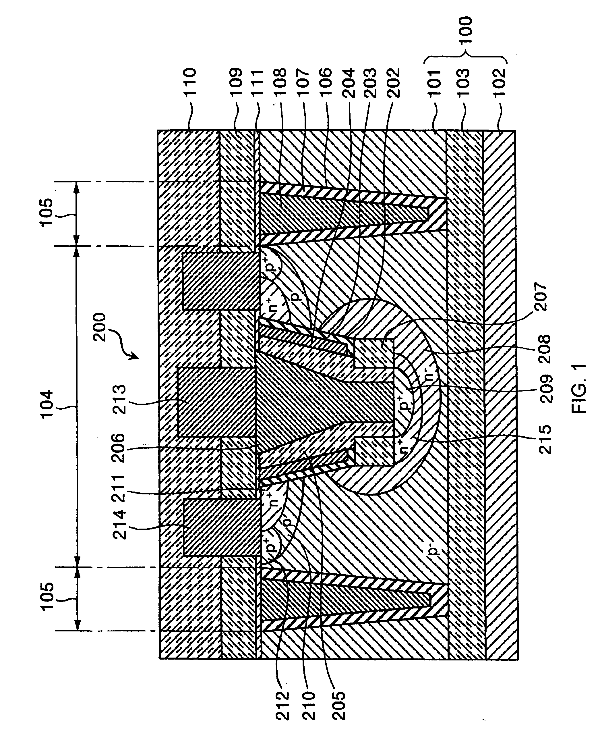
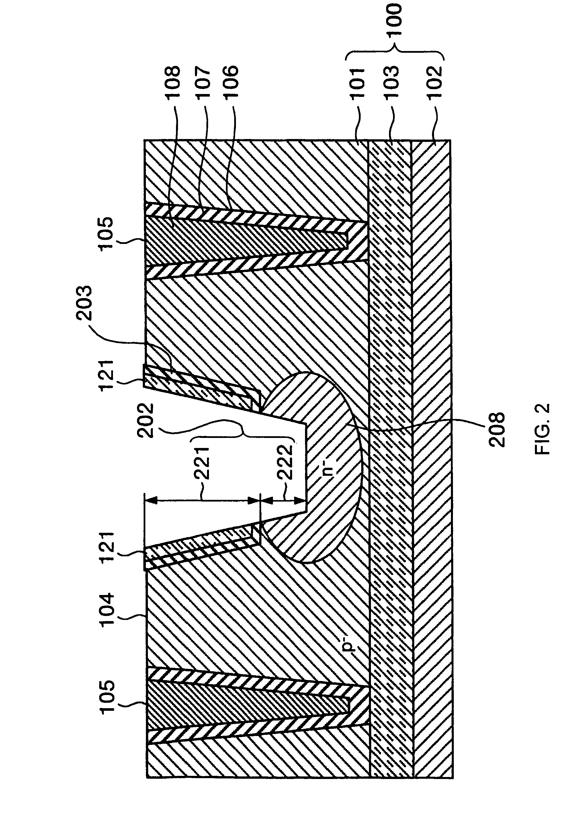
FIG. 1 is a cross-sectional view showing an arrangement of a semiconductor device according to a first mode for carrying out the invention. The semiconductor device of the first mode is a TL-IGBT provided with a collector contact at the bottom of a trench (hereinafter referred to as a TL-IGBT / C). As shown in FIG. 1, the TL-IGBT / C 200 is formed on an SOI substrate 100 with a structure in which a p−-single-crystal silicon semiconductor layer (hereinafter referred to as a p−-semiconductor layer) 101 is formed on an oxide film 103 provided as an insulator layer on the surface of a semiconductor supporting substrate (hereinafter referred to as a supporting substrate) 102.

In the p−-semiconductor layer 101, an element-forming region 104 is formed like an island while being isolated by a trench isolation region 105. The trenc...


PUM


Abstract

A semiconductor structure with device trench and a semiconductor device in the device trench, that enables realization of high integration, lowered on-resistance, reduction in switching losses and a high operation speed in a semiconductor device provided with a lateral IGBT, and that prevents malfunctions such as latchup when IGBTs or an IGBT and CMOS devices are integrated together. The structure includes an SOI substrate having a supporting substrate, an oxide film and a p-semiconductor layer. An island-like element-forming region is isolated by a trench isolation region from surroundings. The trench isolation region includes an isolation trench with an insulation film on its inner wall. The device trench is formed in the element-forming region. A gate electrode is formed with a gate insulator film in the device trench. A collector region and an emitter region outside are provided respectively on the bottom and the outside of the device trench.

Description

BACKGROUND OF THE INVENTION 1. Field of Invention The invention relates to a semiconductor device. More particularly, the invention relates to an insulated gate semiconductor device with low on-resistance, used for a high breakdown voltage IC to control a large current, such as an IC for a switching power source. The invention also relates to an IC for driving an automotive power system and to an IC for a plasma display panel driver. 2. Prior Art In recent years, with the rapid spread of portable information appliances and the development of information technology, power ICs containing power MOSFETs are becoming more important. As for a power IC with a lateral power MOSFET and a control circuit thereof being integrated together, expectations are placed on downsizing, lowered power consumption, increased reliability and reduced cost. This is in contrast to a previous arrangement of a combination of a discrete power MOSFET with control and driving circuits. Thus, on the basis of C...

Claims


Application Information

Patent Timeline
Patent Type & Authority Applications(United States)
IPC IPC(8): H01L21/762H01L21/77H01L21/84H01L27/12H01L29/417H01L29/423H01L29/739
CPCH01L21/76283H01L21/84H01L27/1203H01L29/7394H01L29/4232H01L29/4238H01L29/41766
Inventor SUGI, AKIOFUJISHIMA, NAOTO
Owner FUJI ELECTRIC HLDG CO LTD
Why Eureka
Try Eureka