Multilayer integrated circuit for RF communication and method for assembly thereof

a multi-layer integrated circuit and communication technology, applied in the field of radio frequency (rf) communication, can solve the problems of large area consumed by the inductor, large percentage of costly rf module real estate, and disadvantage to design engineers for developing smaller, efficient heat dissipation properties of handsets, and achieve low profile

Active Publication Date: 2006-11-07
AVAGO TECH KOREA
View PDF12 Cites 33 Cited by
  • Summary
  • Abstract
  • Description
  • Claims
  • Application Information

AI Technical Summary

Problems solved by technology

In general, the passive components are not integrated with the RFIC, and consequently consume large areas of the RF module.
Since the spiral inductor has an inductance value proportional to various physical dimensions including the length of the coil and the number of windings, the inductor may consume a large percentage of costly RF module real estate.
The constraint placed upon the size and configuration of the RF module 100 by the lead frame inductors 140, 150, and 160 is disadvantageous to design engineers for developing smaller, lower cost handsets with efficient heat dissipation properties.
However, manufacturing process steps in the assembly of the multi-PCB layer 320 are complex, and may lead to low yields.
Furthermore, heat flow is unidirectional, and thus restricted, due to layout and configuration of the RFIC 110, lead frame 105, heat sink plate 310, and thermal grease 350.
In fact, if heat is not effectively dissipated, electronic components of the RFIC 110 may be damaged and rendered non-operational.
Since the plastic BGA packaged RF module 200 (FIG. 2) and the thermal enhanced BGA packaged RF module 300 (FIG. 3) dissipate heat in one direction only, heat transfer rates are poor for these designs.

Method used


Image

  • Multilayer integrated circuit for RF communication and method for assembly thereof
  • Multilayer integrated circuit for RF communication and method for assembly thereof
  • Multilayer integrated circuit for RF communication and method for assembly thereof

Examples


Embodiment Construction

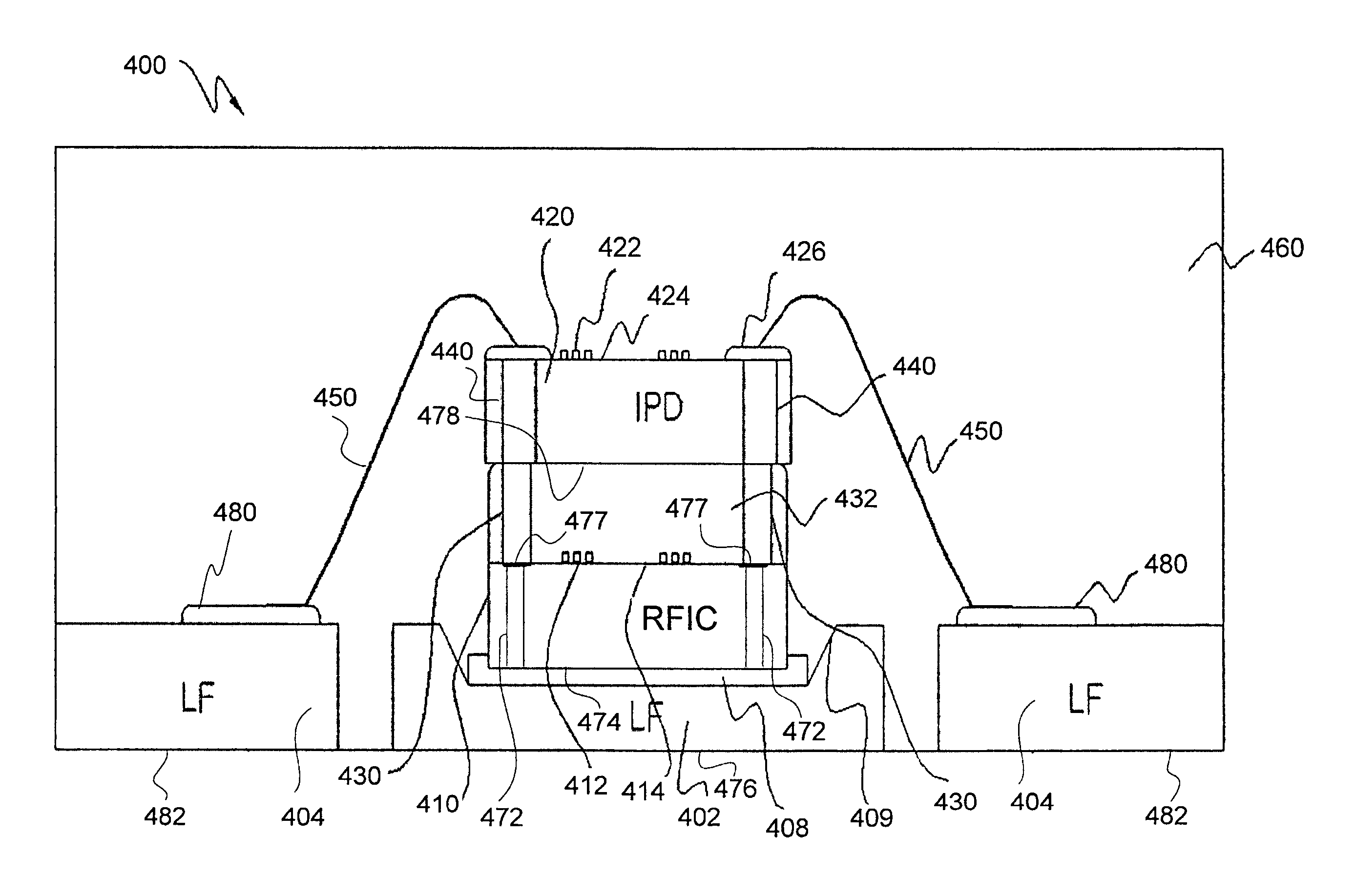
[0026]FIG. 4 illustrates a vertically integrated RF module package 400 according to one embodiment of the present invention. The vertically integrated RF module package 400 comprises an RFIC 410 and an integrated passive device (IPD) 420 stacked on a lead frame 402. The RFIC 410 and the IPD 420 may also be referred to as an RFIC die and an IPD die, respectively. In one embodiment of the present invention, the RFIC 410 is fabricated on a gallium arsenide (GaAs) substrate and the IPD 420 is fabricated on a silicon (Si) substrate. On an upper surface 414 of the RFIC 410, an active integrated circuit pattern 412 is formed. The active integrated circuit pattern 412 comprises active radio frequency circuitry for processing RF signals. The active radio frequency circuitry may include any number or combination of, transistors, power amplifiers, synthesizers, A / D converters, and D / A converters, for example. Similarly, on an upper surface 424 of the IPD 420, a passive integrated circuit patte...


PUM


Abstract

A low profile radio frequency (RF) module and package with efficient heat dissipation characteristics, and a method of assembly thereof, are provided. In some embodiments, the RF module package comprises a radio frequency integrated circuit (RFIC) attached to a recessed area of a lead frame. The RFIC has an active integrated circuit pattern and a plurality of conductors formed on input / output pads of the active integrated circuit pattern. An integrated passive device (IPD) is attached to the RFIC via the plurality of conductors. The IPD has a passive integrated circuit pattern, a plurality of electrode pads connected to nodes of the passive integrated circuit pattern, and metal-filled vias for electrically connecting the electrode pads to the plurality of conductors. The RFIC includes a plurality of heat conducting vias for conducting heat to the lead frame.

Description

CROSS-REFERENCE TO RELATED APPLICATIONS[0001]This application claims priority from Korean Patent Application No. 2004-0020075 by Youngwoo Kwon, entitled “RF Module Package and Assembly Method Thereof,” filed Mar. 24, 2004, the disclosure of which is incorporated by reference herein. This application is related to U.S. application Ser. No. 10 / 932,409 entitled “INTEGRATED CIRCUIT MODULE PACKAGE AND ASSEMBLY METHOD THEREOF” filed on even date herewith.BACKGROUND OF THE INVENTION[0002]1. Field of the Invention[0003]This invention relates generally to radio frequency (RF) communication and more particularly to a multilayer integrated circuit for RF communication and methods for assembly thereof.[0004]2. Description of the Background Art[0005]Cell phone manufacturers are under competitive pressure to make cell phones smaller, less costly, more power efficient, and more sophisticated by adding new functional capabilities. Accordingly, designers may focus on reducing the size and cost of RF...

Claims


Application Information

Patent Timeline
Patent Type & Authority Patents(United States)
IPC IPC(8): H01L23/34H01L23/02H01L23/433H01L23/495H01L23/66H01L25/16H01L29/00
CPCH01L23/4334H01L23/49503H01L23/49589H01L23/66H01L25/165H01L2224/16145H01L2224/48091H01L2224/48227H01L2224/49109H01L2224/49171H01L2224/73253H01L2924/01046H01L2924/01079H01L2924/14H01L2924/15311H01L2924/1532H01L2924/19041H01L2924/30107H01L2924/3011H01L2924/00014H01L24/48H01L24/49H01L2924/00H01L2924/00012H01L2924/10253H01L2224/16265H01L2224/32245H01L2924/19104H01L2924/30111H01L2224/05573H01L2224/05568H01L2224/05624H01L2224/05644H01L2224/05647H01L24/05H01L2224/45099H01L2224/45015H01L2924/207B65F1/1463B65F1/1426B65F2210/132
Inventor KWON, YOUNGWOOCHUNG, KI WOONG
Owner AVAGO TECH KOREA
Why Eureka
Try Eureka