Liquid crystal display

a technology of liquid crystal display and liquid crystal, applied in the field of liquid crystal display, can solve the problem of varying the relative retardation amount, and achieve the effect of widening the viewing angl

Inactive Publication Date: 2006-11-07
SANYO ELECTRIC CO LTD
View PDF7 Cites 5 Cited by
  • Summary
  • Abstract
  • Description
  • Claims
  • Application Information

AI Technical Summary

Benefits of technology

[0009]This invention has been conceived to overcome the above problems and aims to provide a liquid crystal display for achieving a wider viewing angle through appropriate control of the orientation of liquid crystal molecules.

Problems solved by technology

However, even if this angle is primarily controlled by adjusting electric field strength, a relative retardation amount will vary depending on an angle at which an observer views the LCD, i.e., a viewing angle.
This is a problem of view angle dependency of an LCD.

Method used


Image

  • Liquid crystal display
  • Liquid crystal display
  • Liquid crystal display

Examples


embodiment 1

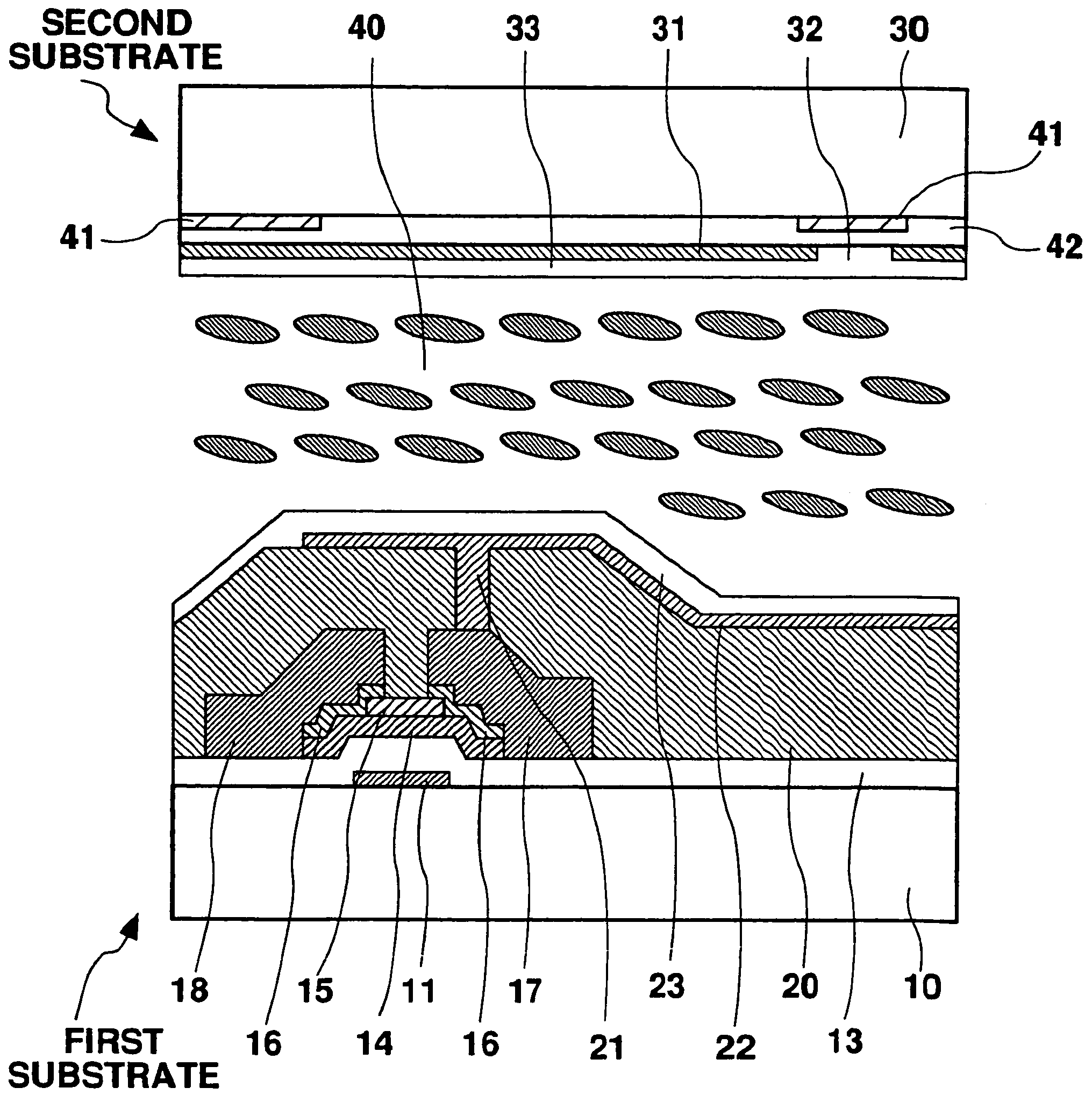
[0042]FIGS. 3 and 4 show the structure of a unit pixel for an LCD according to a first embodiment of the present invention. FIG. 3 is a plane view; FIG. 4 is a cross-sectional view along the line A—A in FIG. 3. A transparent substrate 10 made of glass, etc., is provided. On substrate 10, a conductive film made of Cr, etc., is formed in a predetermined shaped to have a thickness of 1500 Å by means of etching using photo-lithography, whereby a gate electrode 11 and a gate line 12 are constituted. A gate line 12 integrally connects a row of gate electrodes 11 aligned in the same row direction. Covering the whole of substrate 10, a Si3N4 or SiO2 layer is formed having a thickness of 2000 Å to 4000 Å by means of CVD to thereby constitute a gate insulation film 13. On gate insulation film 13, an a-Si layer 14 is formed in a region corresponding to gate electrode 11, so that it will act as an operating layer for the TFT. Amorphous Si regions doped with impurities are formed at both ends of...

embodiment 2

[0066]FIGS. 13 and 14 show a structure of a unit pixel for an LCD according to a second preferred embodiment of the present invention. FIG. 13 is a plane view; FIG. 14 is a cross-sectional view along the line B—B in FIG. 13. Electrode arrangement is almost the same as that in the first embodiment. That is, a TFT substrate first substrate comprises a substrate 50, a gate electrode 51, a gate insulation film 53, an a-Si layer 54, an etching stopper 55, an (N+a-Si) layer 56, and a source and drain electrode 57 / 58, which are layered on the substrate 50 in that order; gate and drain electrodes 51, 58 are formed integral to respective gate and drain lines 52, 59; an inter-layer insulation film 60 is formed covering the TFT and associated respective electrode lines; a pixel electrode 62 is formed on inter-layer insulation film 60, connecting to source electrode 57 via a contact hole 61. An opposing substrate (second substrate) comprising glass substrate 70 is provided opposing to the TFT s...

embodiment 3

[0068]FIGS. 16, 17, 18, and 19 show the structure of a unit pixel for an LCD according to a third preferred embodiment of the present invention. FIG. 16 is a plane view and FIGS. 17, 18, and 19 are respective cross-sectional views along the lines C—C, D—D, and E—E in FIG. 16. In this embodiment, on a substrate 100, a drain electrode 101, a source electrode 102, and a drain line 103 all made of a low resistive metal, such as, Cr, Al, Ta, ITO are formed. Drain electrode 101 and drain line 103 are integrally formed. Above these, an a-Si layer 104 and a gate insulation film 105 are formed in this sequence, forming a gate line 107 made of Al, etc. A part of gate line 107 constitutes a gate electrode 106, which is disposed on the drain electrode 101 and source electrode 102. These together constitute a TFT. Covering the TFT and associated electrode lines, an inter-layer insulation film 108 is provided, with a contact hole CT formed throughout. This film 108 is made of material having plan...


PUM

PropertyMeasurementUnit
thicknessaaaaaaaaaa
thicknessaaaaaaaaaa
dielectric constantaaaaaaaaaa

Abstract

A liquid crystal display is disclosed in which a TFT is formed by forming on a substrate (10), a gate electrode (11), a gate insulation film (13), an a-Si layer (14), an etching stopper (15), an (N+a-Si) layer (16), a source electrode (17), and a drain electrode (18) in this sequence. Covering this TFT, an inter-layer insulation film (20) is formed, on which a pixel electrode (22) is then formed. In a common electrode (31), there is formed an orientation control window (32) where no electrodes are situated. With this arrangement, it is possible to prevent the orientation of liquid crystal molecules from being disturbed due to the influence of electric fields generated by the gate electrode (11), the drain electrode (18), or their respective associated lines. As a result, the orientation of liquid crystal molecules is effectively controlled through electric fields generated in the sloped direction around the edges of the pixel electrode (22) and orientation control window (32), thereby obtaining preferable pixel dividing and a wider range of visibility.

Description

[0001]This is a continuation of application Ser. No. 09 / 721,056 filed Nov. 22, 2000, now U.S. Pat. No. 6,747,721, which application is hereby incorporated by reference in its entirety.BACKGROUND OF THE INVENTION[0002]1. Field of the Invention[0003]The present invention relates to a liquid crystal display (LCD) utilizing the electro-optical anisotropy of liquid crystal, and in particular, to an LCD for achieving a high aperture ratio and a wide viewing angle.[0004]2. Description of the Prior Art[0005]The LCD is advantageous in that it is small and light-weight, and has low power consumption. It is thus put into practical use in such fields as in OA and AV equipment. In particular, the active matrix type which uses a thin film transistor (TFT) for the switching element can, in principle, perform static drive of 100% duty ratio in a multiplexed manner, and is used for large screen, animation displays.[0006]FIGS. 1 and 2 show the structure of a unit pixel for a conventional LCD; FIG. 1 ...

Claims


Application Information

Patent Timeline
Patent Type & Authority Patents(United States)
IPC IPC(8): G02F1/1343G02F1/136G02F1/1333G02F1/1337G02F1/1368G02F1/139H01L29/786
CPCG02F1/133753G02F1/133707G02F1/1393G02F2001/133357G02F1/133357
Inventor KOMA, NORIO
Owner SANYO ELECTRIC CO LTD
Why Eureka
Try Eureka