Spin readout and initialization in semiconductor quantum dots

a quantum dot and readout technology, applied in the field of semiconductor quantum dot devices, can solve the problems of preparing, storing and measuring spins, and particular challenges in measuring spin qubits, and achieve the effect of rapid initialization of the spin sta

Active Publication Date: 2006-11-14
WISCONSIN ALUMNI RES FOUND
View PDF8 Cites 16 Cited by
  • Summary
  • Abstract
  • Description
  • Claims
  • Application Information

AI Technical Summary

Benefits of technology

[0008]In accordance with the present invention, spin information is converted to charge information in a semiconductor quantum dot and a single electron sensitive electrometer such as a single electron transistor is used to read out the resulting charge or orbitals in the quantum dot. Both readout and rapid initialization of the spin state can be achieved. Rapid initialization (as compared to initialization by thermalization) is carried out in a manner that obviates the need for spin-polarized leads or ancillary qubits.
[0009]The present invention may be incorporated in various material systems, such as GaAs / AlGaAs and a Si / SiGe heterostructure, in which the active layer is pure strained Si, which minimizes decoherence from spin-phonon coupling. The qubits are gated quantum dots which hold one electron, with a gate geometry which confines the electrons in asymmetric lateral wells, such that orbital excitation results in lateral center-of-charge movement. A magnetic field having a gradient along the length of the quantum dot can be utilized to provide spin state splitting of differing energies in the two orbitals of the electron to facilitate selective excitement of the spin orientation.

Problems solved by technology

Potential issues with such proposed systems include individual impurity spins, as well as gate operation and readout methods for the quantum dots.
However, the combined challenge of preparing, storing and measuring spins is formidable.
The measurement of spin qubits is a particular challenge.

Method used


Image

  • Spin readout and initialization in semiconductor quantum dots
  • Spin readout and initialization in semiconductor quantum dots
  • Spin readout and initialization in semiconductor quantum dots

Examples


Embodiment Construction

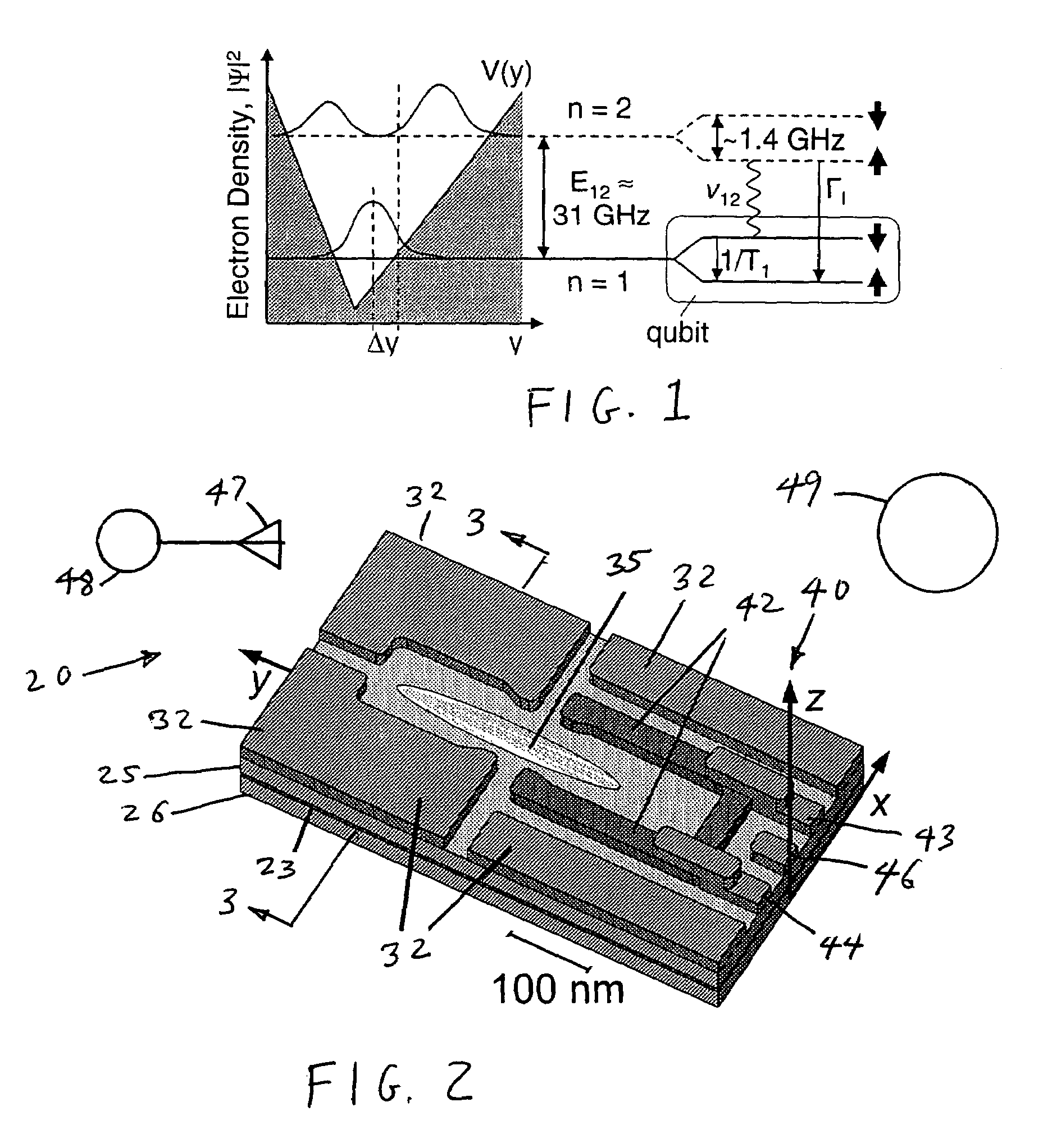
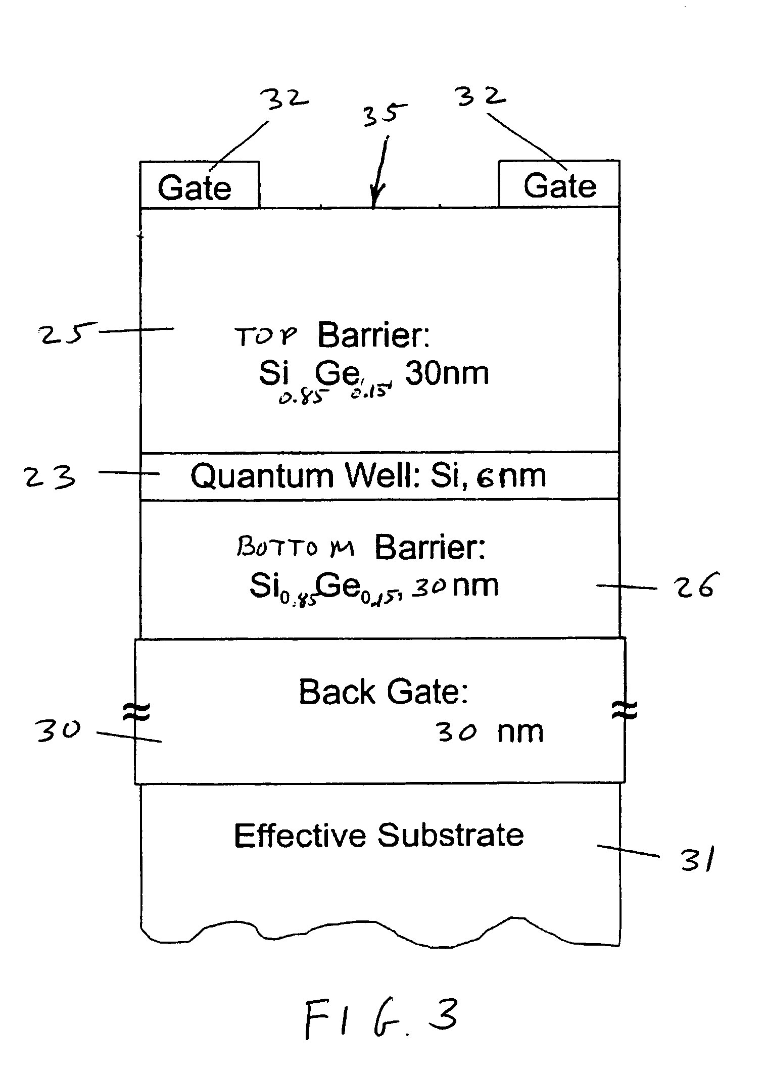
[0022]The present invention may be implemented in various semiconductor material systems. For example only, these material systems include, but are not limited to, Si / SiGe and GaAs—AlGaAs heterostructures, as described in M. Friesen, et al., Phys. Rev. B67, 121301(R) (2003), and in U.S. Pat. No. 6,597,010, incorporated herein by reference. In the Si / SiGe system, the active layer is pure strained Si, which minimizes decoherence from spin-phonon coupling as discussed in C. Tahan, et al., Phys. Rev. B66, 035314 (2002).

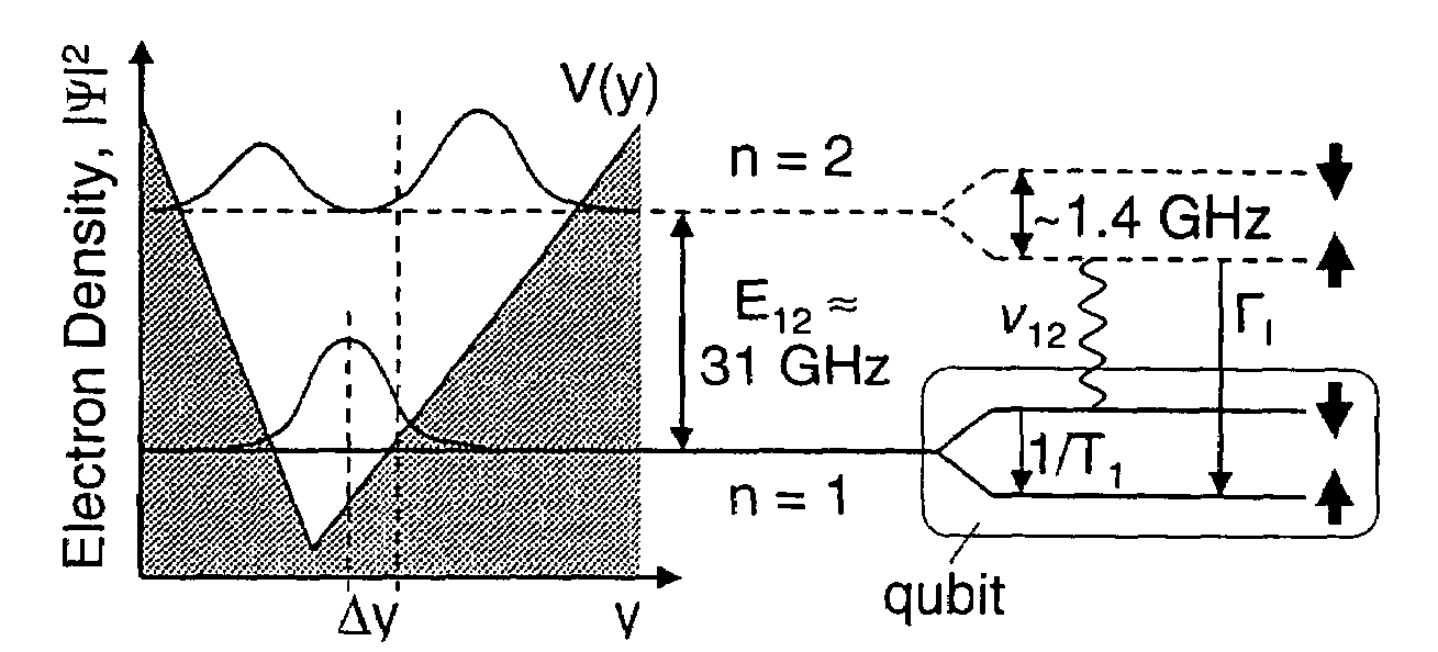
[0023]In the present invention, the electrons are confined in asymmetric lateral wells, such that orbital excitation results in lateral center-of-charge movement. FIG. 1 shows the first two orbital states of an electron confined to an asymmetric quantum dot, with center-of-charge positions varying by a distance Δy. If an external microwave radiation source of frequency E12 / h (where h is Planck's constant), having an energy corresponding to the difference in energy between...


PUM


Abstract

A semiconductor quantum dot device converts spin information to charge information utilizing an elongated quantum dot having an asymmetric confining potential along its length so that charge movement occurs during orbital excitation. A single electron sensitive electrometer is utilized to detect the charge movement. Initialization and readout can be carried out rapidly utilizing RF fields at appropriate frequencies.

Description

STATEMENT OF GOVERNMENT RIGHTS[0001]This invention was made with United States government support awarded by the following agencies: Army / MRMC DAAD19-01-1-0515. The United States government has certain rights in this invention.FIELD OF THE INVENTION[0002]This invention pertains generally to the field of semiconductor devices and particularly to semiconductor quantum dot devices that may be utilized in quantum computing.BACKGROUND OF THE INVENTION[0003]Quantum computing utilizes quantum particles to carry out computational processes. The fundamental unit of quantum information is called a quantum bit or qubit. A qubit can be both a zero and a one at the same time. An example is the spin of an electron, wherein the up or down spin can correspond to a zero, a one, or a superposition of states in which it is both up and down at the same time. Performing a calculation using the electron essentially performs the operation simultaneously for both a zero and a one. Experimental advances in ...

Claims


Application Information

Patent Timeline
Patent Type & Authority Patents(United States)
IPC IPC(8): H01L29/06H01L29/12H01L29/66
CPCB82Y10/00H01L29/127H01L29/66984
Inventor FRIESEN, MARK GREGORYTAHAN, CHARLES GEORGEJOYNT, ROBERT JAMESERIKSSON, MARK A.
Owner WISCONSIN ALUMNI RES FOUND
Why Eureka
Try Eureka