Semiconductor device

a semiconductor and memory technology, applied in the field of memory devices, can solve the problems of large capacity of high access speed memory, data stored in cache memory cannot be specified immediately after, and the time for invalidation of valid bits cannot be reduced, so as to achieve low power consumption of the cpu, high speed, and low cost

Inactive Publication Date: 2008-10-28
SEMICON ENERGY LAB CO LTD
View PDF13 Cites 12 Cited by
  • Summary
  • Abstract
  • Description
  • Claims
  • Application Information

AI Technical Summary

Benefits of technology

[0012]The invention provides a cache memory having valid bits, where a circuit configuration in a memory cell of a valid bit is improved so as to perform invalidation at high speed.
[0034]According to the invention, in a cache memory having valid bits, all the valid bits can be invalidated at the same time; therefore, the invalidation of the valid bits are carried out at high speed. In other words, the time for invalidation of valid bits can be reduced, and the CPU can have access to the cache memory without being put in standby mode.
[0035]Such a memory array can be used as a cache memory of a CPU (Central Processing Unit) or an MPU (Micro Processing Unit). By applying the memory array, low power consumption of the CPU or the MPU can be achieved. Furthermore, when a reset signal is outputted in synchronism with power supply, a cache memory can be initialized quickly, leading to improvement in processing speed of the CPU. That is to say, the time for initial setting of the cache memory can be significantly reduced so that the CPU can perform the processing efficiently. As a result, a semiconductor device with excellent processing performance can be provided.

Problems solved by technology

However, this architecture has a problem in an access speed to the memory.
It is difficult, however, to use a high access speed memory having a large capacity since a high access speed memory is expensive.
This is because the cache memory, which is generally constituted by an SRAM (Static Random Access Memory), cannot hold data when a power supply is off, and thus data stored in the cache memory cannot be specified immediately after a power supply is turned on.
However, this invalidation of valid bits takes time since it is performed for each line.
After the invalidation is completed, the required data is immediately stored in a cache memory, which results in high speed operation of the cache memory.

Method used


Image

  • Semiconductor device
  • Semiconductor device
  • Semiconductor device

Examples


embodiment mode 1

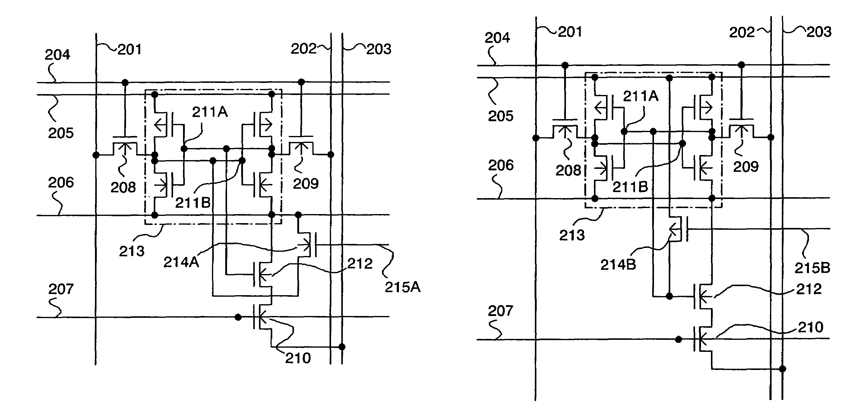
[0048]A memory cell configuration that allows invalidation of valid bits in a cache memory to be performed at high speed is described with reference to FIGS. 1A to 3 and FIGS. 6 to 7B. Although the description is made using a power supply voltage of 5 V, the invention is not limited to this.

[0049]FIGS. 1A and 1B are circuit diagrams each showing a memory cell configuration of a valid bit in a cache memory according to this embodiment mode. In FIGS. 1A and 1B, a memory cell includes a power supply line 205, a ground line 206, a word line for writing 204, a word line for reading 207, a data line for writing 201, a data line for writing 202, a data line for reading 203, an N-channel transistor 208, an N-channel transistor 209, an N-channel transistor 210, an N-channel transistor 212, an N-channel transistor 214A, and an inverter circuit 213. The inverter circuit 213 includes two inverters. Writing data is inputted to the data line for writing 201, while inverted data thereof is inputte...

embodiment mode 2

[0065]In this embodiment mode, a different mode than Embodiment Mode 1 is described with reference to FIGS. 4A and 4B. FIGS. 4A and 4B are circuit diagrams each showing a memory cell configuration of a valid bit of a cache memory according to Embodiment Mode 2 of the invention. Basically, FIG. 4A has a similar configuration to FIG. 1A and FIG. 4B has a similar configuration to FIG. 7A; however, a resistor 217 is used instead of the N-channel transistor 214A as an element for the invalidation of valid bits. The resistor 217 preferably has a resistance value of several hundreds kΩ to several MΩ.

[0066]According to the circuit configurations shown in FIGS. 4A and 4B, the potential of the node 211B is fixed to 0 V by the resistor 217 even when a power supply is off. Since the potential of the node 211B is also 0 V when the power supply is on, the memory cell of a valid bit holds ‘0’. This is in the same state in which the invalidation of valid bits is performed. In that case, normal writ...

embodiment mode 3

[0072]In this embodiment mode, a different mode than Embodiment Modes 1 and 2 is described with reference to FIGS. 5A and 5B. FIGS. 5A and 5B are circuit diagrams each showing a memory cell configuration of a valid bit of a cache memory according to Embodiment Mode 3 of the invention. Basically, FIG. 5A has a similar configuration to FIG. 1A and FIG. 5B has a similar configuration to FIG. 7A; however, a capacitor 218 is used instead of the N-channel transistor 214A as an element for the invalidation of valid bits. The capacitance of the capacitor 218 is required to be determined such that the sum of the wiring capacitance of the node 211B and the capacitance of the capacitor 218 is larger than the sum of the wiring capacitance of the node 211A and the wiring capacitance of the N-channel transistor 212 for reading, so as to upset the balance between them. However, when the sum of the wiring capacitance of the node 211B and the capacitance of the capacitor 218 is too large, writing op...


PUM


Abstract

A cache memory having valid bits, where a circuit configuration in a memory cell of a valid bit is improved so as to perform invalidation at high speed. The invention provides a cache memory including a memory cell that has a function to perform invalidation at high speed. One mode of the invention is a semiconductor device including a memory cell of a valid bit, where two inverters are connected in series to form a loop, a drain of an N-channel transistor is connected to an output signal line of one of the inverters, a gate thereof is connected to a reset signal line of a CPU, and a source thereof is connected to a ground line. The initial value of the memory cell is determined by inputting a reset signal of the CPU to the gate.

Description

BACKGROUND OF THE INVENTION[0001]1. Field the Invention[0002]The present invention relates to a memory device mounted on a semiconductor device and a semiconductor device including the memory device. Specifically, the invention relates to a cache memory device having valid bits.[0003]2. Description of the Related Art[0004]Almost all the current central processing units (CPUs) are based on an architecture called the stored program system. According to this stored program system, instructions processed by a CPU and data necessary for the processing are stored in a memory, and the processing of the CPU is carried out by sequentially reading data from the memory.[0005]However, this architecture has a problem in an access speed to the memory. As storing instructions processed by the CPU and data necessary for the processing, the memory is required to have a large capacity. It is difficult, however, to use a high access speed memory having a large capacity since a high access speed memory...

Claims


Application Information

Patent Timeline
Patent Type & Authority Patents(United States)
IPC IPC(8): G11C11/00G11C5/06
CPCG06F12/0891G11C11/412H01L27/1203H01L27/11H01L27/1108H01L21/84G06F12/0895H10B10/125H10B10/00
Inventor FUJITA, MASASHIKUROKAWA, YOSHIYUKI
Owner SEMICON ENERGY LAB CO LTD
Why Eureka
Try Eureka