Heterojunction bipolar transistor having reduced driving voltage requirements

a technology of heterojunction bipolar transistor and driving voltage, which is applied in the manufacture of semiconductor/solid-state devices, semiconductor devices, electrical apparatus, etc., can solve the problems of deteriorating characteristics, deteriorating electric characteristics, and deteriorating high-frequency characteristics of hbt, so as to improve high-frequency characteristics, reduce the recombination current of the emitter-base, and reduce the effect of low-voltage driving

Inactive Publication Date: 2006-11-14
PANNOVA SEMIC
View PDF23 Cites 3 Cited by
  • Summary
  • Abstract
  • Description
  • Claims
  • Application Information

AI Technical Summary

Benefits of technology

[0014]An object of the present invention is providing a heterojunction bipolar transistor in which the emitter-base recombination current is reduced, low-voltage driving is attained, and the high-frequency characteristics are improved.

Problems solved by technology

This deteriorates the electric characteristics.
This HBT however has a problem that an impurity contained in the base region diffuses into the collector region during heat treatment, forming a so-called parasitic barrier between the base and the collector (J. W. Slotboom, G. Streutker, A. Pruijmboom and D. J. Gravesteijn, IEEE Electron Device Letters 12, p.
However, the conventional SiGeC HBT utilizing SiGeC / Si heterojunction has the following problems.
However, according to experiments carried out by the present inventors, it has been found that the high-frequency characteristics of a HBT deteriorate when the C content is increased.
As a result, the characteristics deteriorate.
That is, a short recombination lifetime causes deterioration of the transistor characteristics.

Method used


Image

  • Heterojunction bipolar transistor having reduced driving voltage requirements
  • Heterojunction bipolar transistor having reduced driving voltage requirements
  • Heterojunction bipolar transistor having reduced driving voltage requirements

Examples


embodiment 1

[0056]FIG. 3A is a view showing the C content, the Ge content, and the concentration of boron (B) as an impurity, of the first and second base regions in Embodiment 1. FIG. 3B is an energy band diagram over the emitter region—base region—collector region during voltage application in Embodiment 1. Note that in FIG. 3A, representation of the concentration of an n-type impurity is omitted.

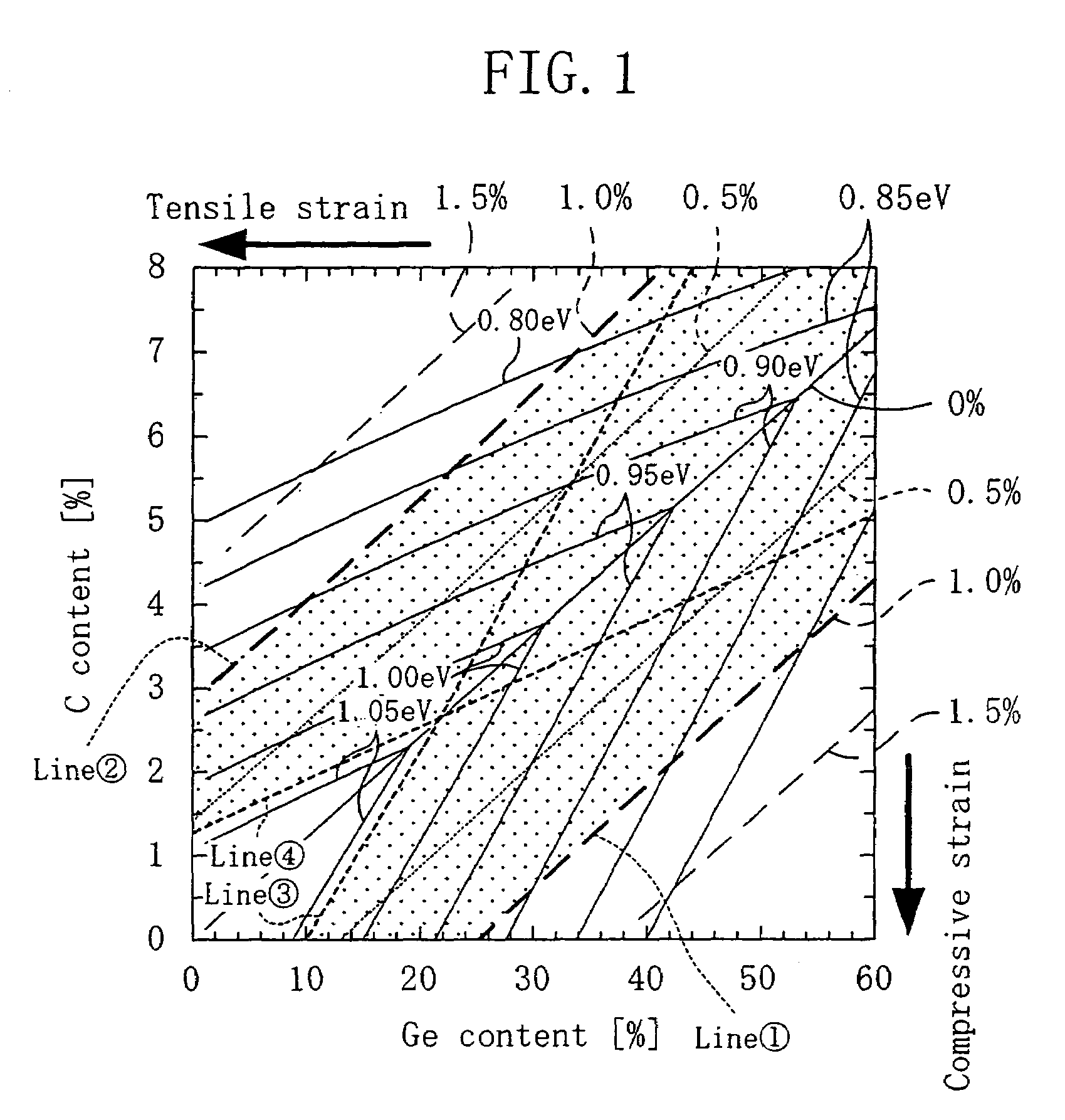
[0057]As shown in FIG. 3A, in this embodiment, the Ge content is constant (for example, 26.8%) throughout the first base region 12 and the second base region 13. The C content is 0.91% in the first base region 12 and 0.35% in the second base region 13, for example. In this case, therefore, the first base region 12 is made of a SiGe0.268C0.0091 layer, while the second base region 13 is made of a SiGe0.268C0.0035 layer.

[0058]The band gap of the SiGe0.268C0.0091 layer is about 0.95 eV, while the band gap of the SiGe0.268C0.0035 layer is about 0.92 eV. When two SiGeC layers having the same Ge content are...

embodiment 1 -

-Experiment Data in Embodiment 1-

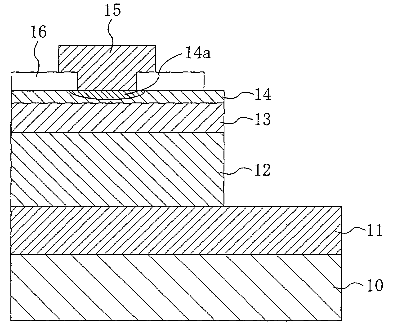
[0060]FIG. 12 is a view, shown in the form of a table, of parameters of samples used for experiments for confirmation of the effects of the present invention. In FIG. 12, S denotes the thickness of the Si cap layer 14, D1 denotes the thickness of the first base region 12, D2 denotes the thickness of the second base region 13. NG1, NC1, and NB1 respectively denote the Ge content, the C content, and the boron concentration of the first base region 12. NG2, NC2, and NB2 respectively denote the Ge content, the C content, and the boron concentration of the second base region 13.

[0061]FIG. 13 is a view showing data of bias voltage-current characteristics measured for the samples shown in FIG. 12. As is found from FIG. 13, in sample No. 1 that does not include a layer having a low C content (second base region), the gradient of the voltage-current characteristics is slow, indicating that the recombination current is large. In sample No. 2 in which the thick...

embodiment 2

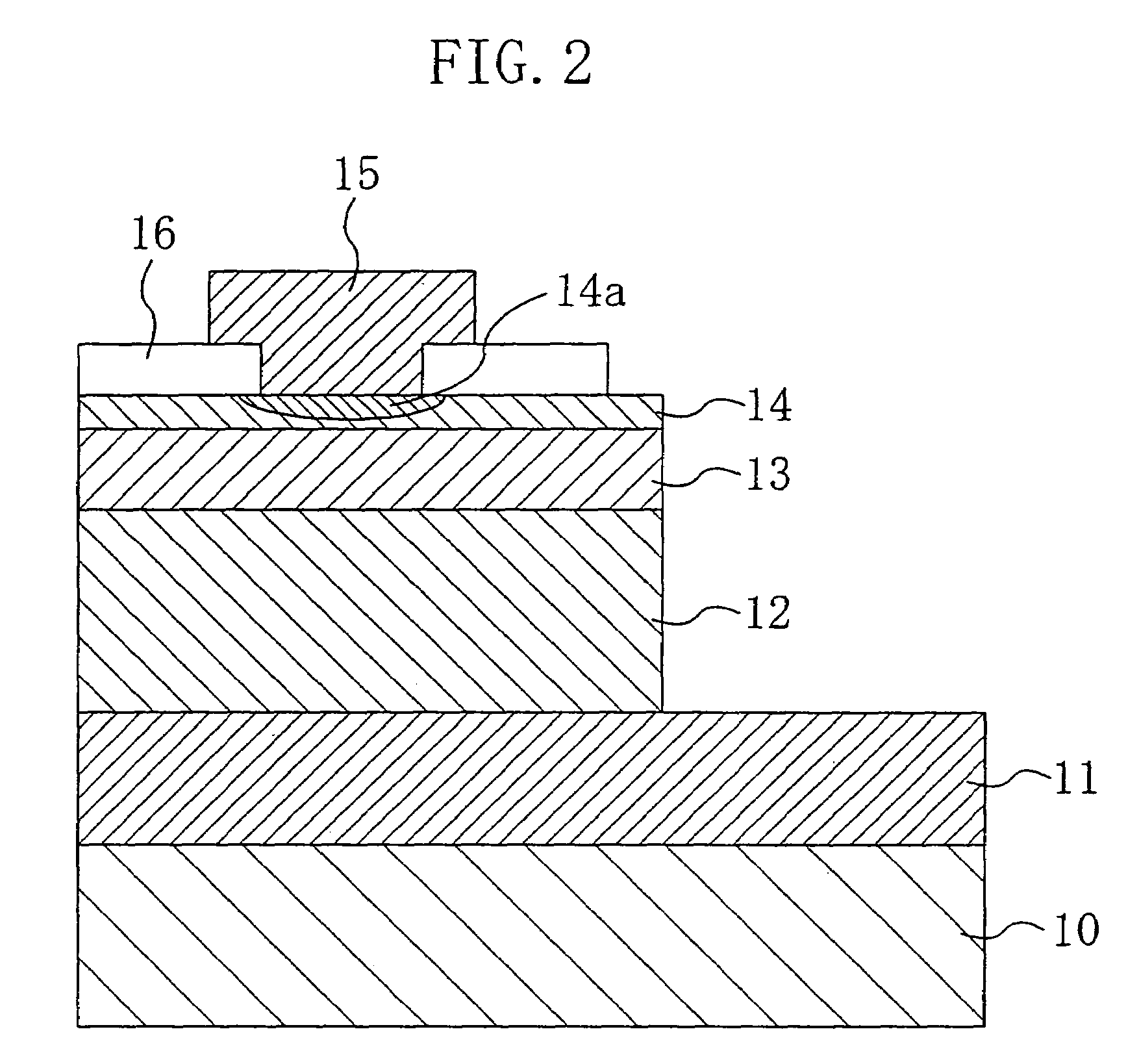
[0063]FIG. 4A is a view showing the C content, the Ge content, and the concentration of boron (B) as an impurity, of the first and second base regions in Embodiment 2. FIG. 4B is an energy band diagram over the emitter region—base region—collector region during voltage application in Embodiment 2. Note that in FIG. 4A, representation of the concentration of an n-type impurity is omitted.

[0064]In this embodiment, the Ge and C contents of the first and second base regions 12 and 13 have been adjusted so that the band gaps of the two base regions are equal to each other. To attain this, the Ge content is not made constant throughout the first and second base regions, but the Ge content of the first base region 12 should be larger than that of the second base region 13. Specifically, when the SiGeC layer is represented by general formula Si1-x-yGexCy and the difference of the C content between the first and second base regions 12 and 13 is denoted by Δy, the difference Δx of the Ge cont...


PUM


Abstract

The bipolar transistor of the present invention includes a Si collector buried layer, a first base region made of a SiGeC layer having a high C content, a second base region made of a SiGeC layer having a low C content or a SiGe layer, and a Si cap layer 14 including an emitter region. The C content is less than 0.8% in at least the emitter-side boundary portion of the second base region. This suppresses formation of recombination centers due to a high C content in a depletion layer at the emitter-base junction, and improves electric characteristics such as the gain thanks to reduction in recombination current, while low-voltage driving is maintained.

Description

[0001]This application is a divisional of application Ser. No. 10 / 461,364 filed Jun. 16, 2003, now U.S. Pat. No. 6,759,697, which is a divisional of Ser. No. 09 / 948,112, filed Sep. 7, 2001 now abandoned, and also claims the benefit of JP 2000-274877 filed on Sep. 11, 2000 in Japan under 35 U.S.C. § 119.BACKGROUND OF THE INVENTION[0002]The present invention relates to a heterojunction bipolar transistor using a semiconductor layer including silicon, and in particular, relates to measures taken to reduce the driving voltage of the heterojunction bipolar transistor.[0003]Conventionally, a heterojunction bipolar transistor (HBT) has attracted attention as a high-function element. The HBT is a transistor in which the compositions of an emitter and a base are determined to ensure that the band gap of the emitter is larger than that of the base, to thereby substantially improve the injection efficiency of the emitter and thus improve the characteristics of the transistor. The HBT, which is...

Claims


Application Information

Patent Timeline
Patent Type & Authority Patents(United States)
IPC IPC(8): H01L29/739H01L31/0328H01L31/0336H01L31/072H01L31/109H01L29/737
CPCH01L29/7378H01L29/737
Inventor TOYODA, KENJIYUKI, KOICHIROTAKAGI, TAKESHIOHNISHI, TERUHITOKUBO, MINORU
Owner PANNOVA SEMIC
Why Eureka
Try Eureka