Temperature dependent semiconductor module connectors

a technology of temperature-dependent semiconductor modules and connectors, which is applied in the direction of fixed connections, coupling device connections, securing/insulating coupling contact members, etc., can solve the problems of difficult factory rework processes, affecting the reliability of assembled modules, and not easily replacing soldered interconnection schemes

Inactive Publication Date: 2006-11-21
IBM CORP
View PDF4 Cites 8 Cited by
  • Summary
  • Abstract
  • Description
  • Claims
  • Application Information

AI Technical Summary

Problems solved by technology

At present, such capability is problematic for organic packages, since the actuation loads required in currently available removable solutions exert forces which are incompatible with the organic module structures.
Soldered interconnection schemes are not readily replaceable and factory rework processes are difficult and may impact the reliability of the assembled module, particularly in a Pb-free soldering environment.
Pin Grid Array interconnects or BGA sockets do provide for more convenient module replacement but can be expensive and often impart changes to electrical parameters, such as increased inductance, that negatively impact device performance.
Moreover, these solutions may not be compatible with 1 mm grid I / O pitch.
The drawback here is, in order to establish reliable connections between the module and circuit board, a substantial force (roughly proportional to the number of module pads) must be applied to the interposer / module assembly.
The required actuation force is typically excessive for organic semiconductor packages.
The high stresses imposed on the laminate substrate structures can cause reliability concerns associated with resin cracks, warpage, inner plane separation and PTH fractures.

Method used


Image

  • Temperature dependent semiconductor module connectors
  • Temperature dependent semiconductor module connectors
  • Temperature dependent semiconductor module connectors

Examples


Embodiment Construction

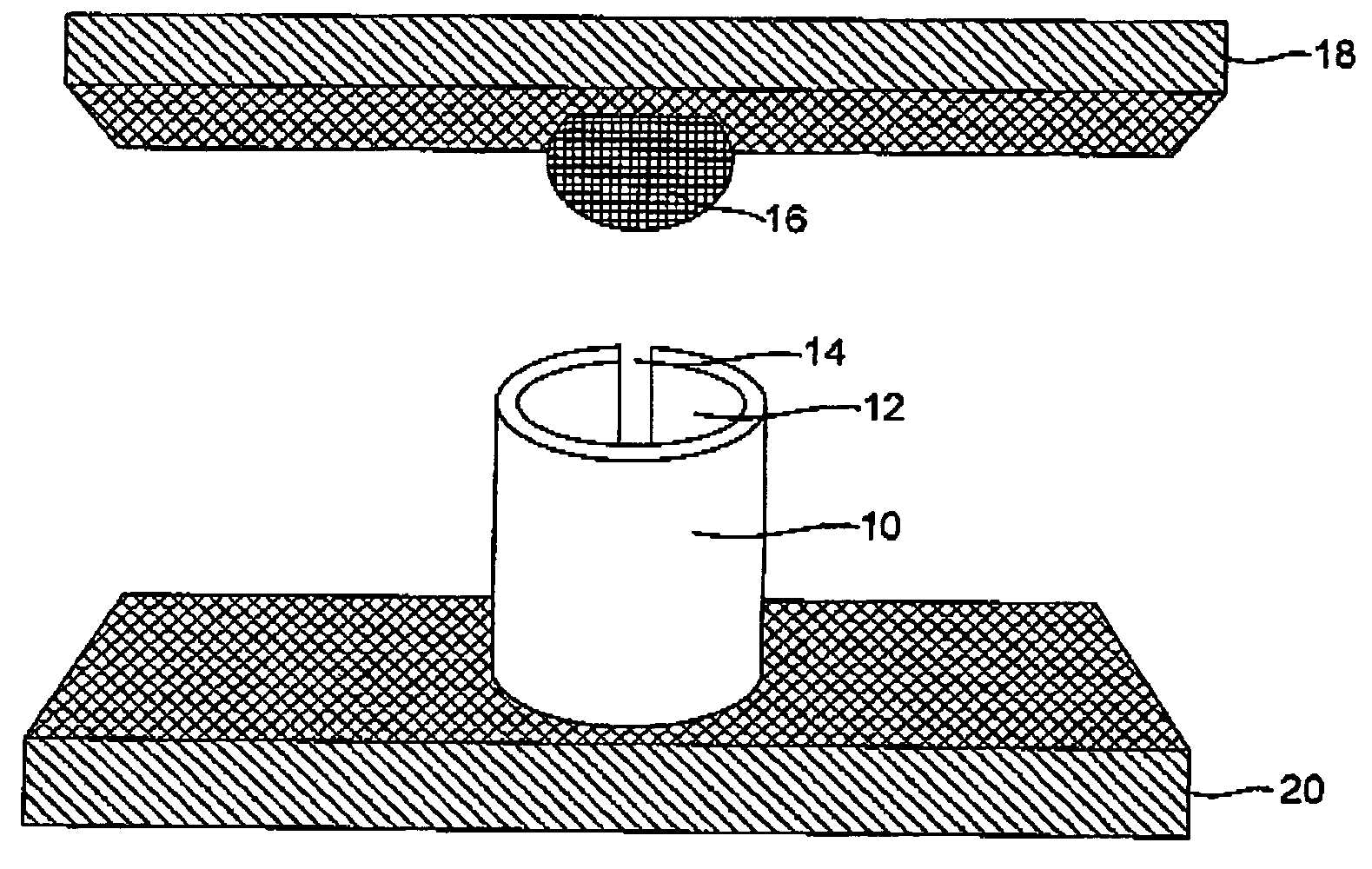
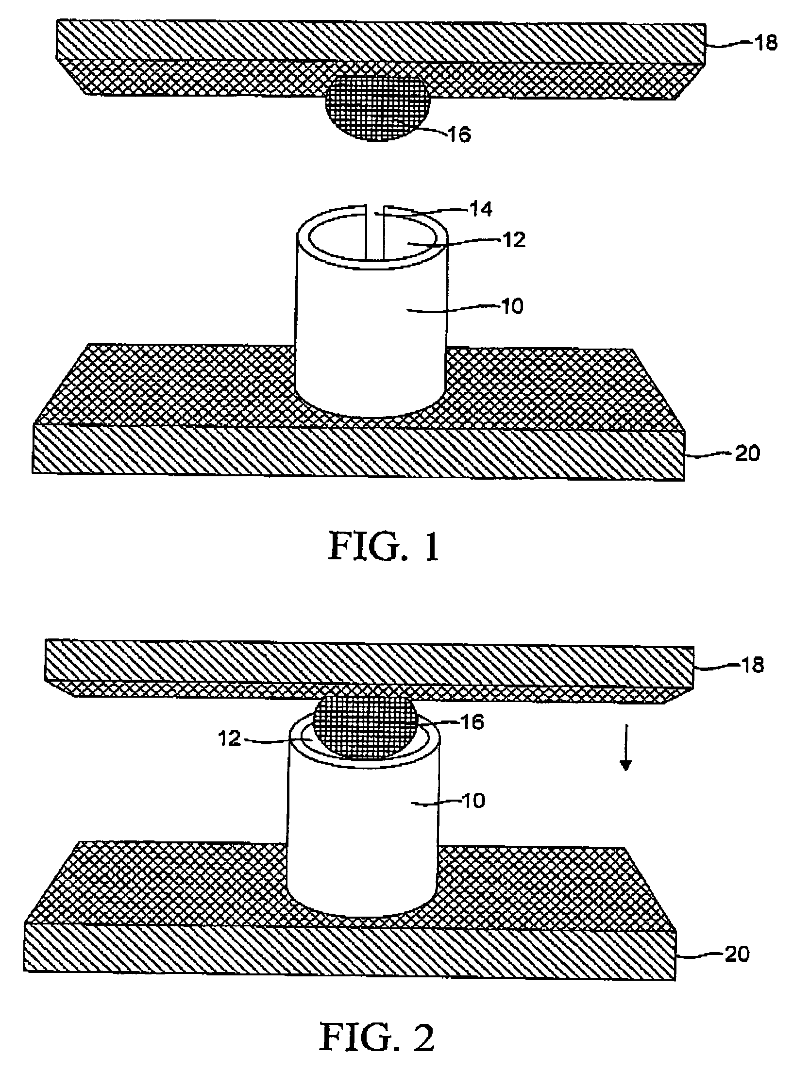
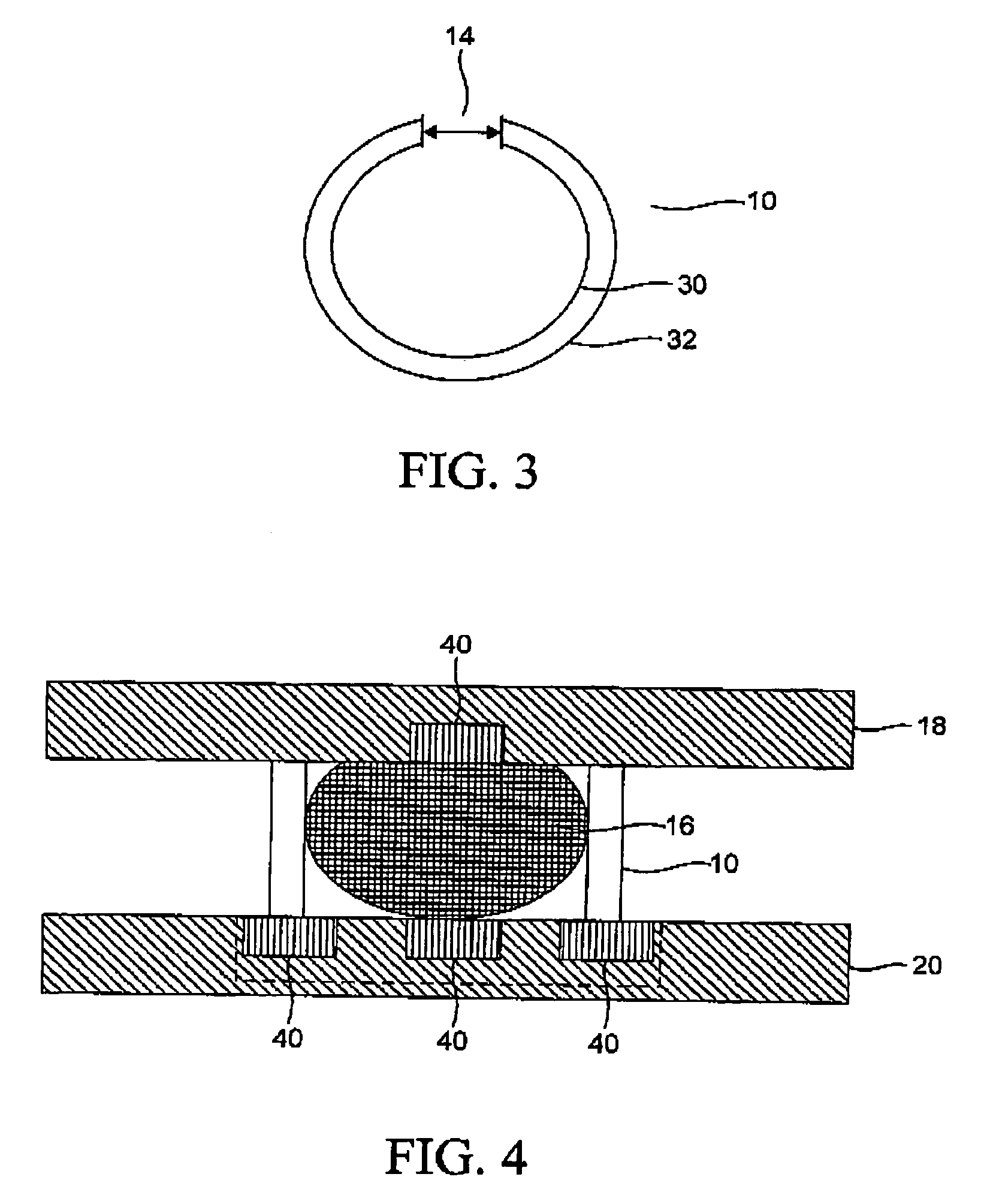
[0029]The present invention and the various features and advantageous details thereof are explained more fully with reference to the nonlimiting embodiments that are illustrated in the accompanying drawings and detailed in the following description. It should be noted that the features illustrated in the drawings are not necessarily drawn to scale. Descriptions of well-known components and processing techniques are omitted so as to not unnecessarily obscure the present invention. The examples used herein are intended merely to facilitate an understanding of ways in which the invention may be practiced and to further enable those of skill in the art to practice the invention. Accordingly, the examples should not be construed as limiting the scope of the invention.

[0030]In order to overcome the problems discussed above, the invention presents an interconnection for use between substrates (such as silicon, ceramic, organic, etc. substrates 18, 20 shown in FIG. 1). These substrates 18, ...


PUM


Abstract

A method and structure is disclosed for forming a removable interconnect for semiconductor packages, where the connector is adapted to repeatedly change from a first shape into a second shape upon being subjected to a temperature change and to repeatedly return to the first shape when not being subjected to the temperature change. The connector can be disconnected when the connector is in its second shape and the connector cannot be disconnected when the connector is in its first shape.

Description

BACKGROUND OF THE INVENTION[0001]1. Field of the Invention[0002]This invention details a method and structure for forming a removable interconnect for semiconductor packages, where the connector is adapted to repeatedly change from a first shape into a second shape upon being subjected to a temperature change and to repeatedly return to the first shape when not being subjected to the temperature change, and where the connector can be disconnected when the connector is in its second shape and the connector cannot be disconnected when the connector is in its first shape.[0003]2. Description of the Related Art[0004]Due to the high cost of semiconductors, circuit boards and systems it is desirable to provide for a method to be able to remove a semiconductor module from an assembled circuit board without damaging the board or module and thereby enable field replacement capability. At present, such capability is problematic for organic packages, since the actuation loads required in curre...

Claims


Application Information

Patent Timeline
Patent Type & Authority Patents(United States)
IPC IPC(8): H01R12/00
CPCH01L23/49811H01L24/72H01R4/01H05K3/325H01R12/52H01L2924/01015H01L2924/01082H01L2924/12044H01L2924/14H01L2924/30107H05K2201/068H05K2201/209H05K2203/1105H01L2224/16237H01L2224/81191H01L2224/81193H01L2224/81141H01L2924/01006H01L2924/01033H01L24/16H01L24/81H01L2224/05026H01L2224/05548H01L2224/0501H01L2224/056H01L2924/00014H01L2224/05011H01L24/05H01L2224/05099
Inventor BRODSKY, WILLIAM L.BUSBY, JAMES A.CHAMBERLIN, BRUCE J.FERRILL, MITCHELL G.SUSKO, ROBIN A.WILCOX, JAMES R.
Owner IBM CORP
Why Eureka
Try Eureka