Semiconductor device and method for manufacturing the same

a technology of semiconductor devices and semiconductors, applied in semiconductor devices, semiconductor/solid-state device details, electrical apparatus, etc., can solve the problems of increased heat generation, poor heat dissipation characteristics, and increased power consumption, and achieve excellent heat dissipation characteristics and high reliability

Active Publication Date: 2006-11-21
TESSERA ADVANCED TECH
View PDF15 Cites 69 Cited by
  • Summary
  • Abstract
  • Description
  • Claims
  • Application Information

AI Technical Summary

Benefits of technology

[0028]The present invention is intended to solve the above-mentioned conventional problems. It is an object of the present invention to provide a semiconductor device with excellent

Problems solved by technology

By the way, when the semiconductor device with such a large scale is operated at high speed, an increase in power consumption is inevitable, which results in increased heat generation.
Although the chip-on-chip method is suitable for the manufacture of a high-performance semiconductor device with a large scale as described above, a semiconductor device manufactured by this method has a problem in that the heat dissipation characteristics thereof are not very good because a plurality of stacked semiconductor chips are encapsulated in encapsulation resin.
Thus, when such a semiconductor device is used in electronic equipment su

Method used


Image

  • Semiconductor device and method for manufacturing the same
  • Semiconductor device and method for manufacturing the same
  • Semiconductor device and method for manufacturing the same

Examples


embodiment 1

(Embodiment 1)

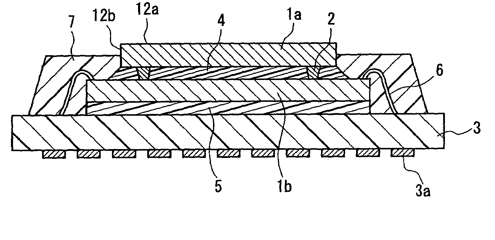
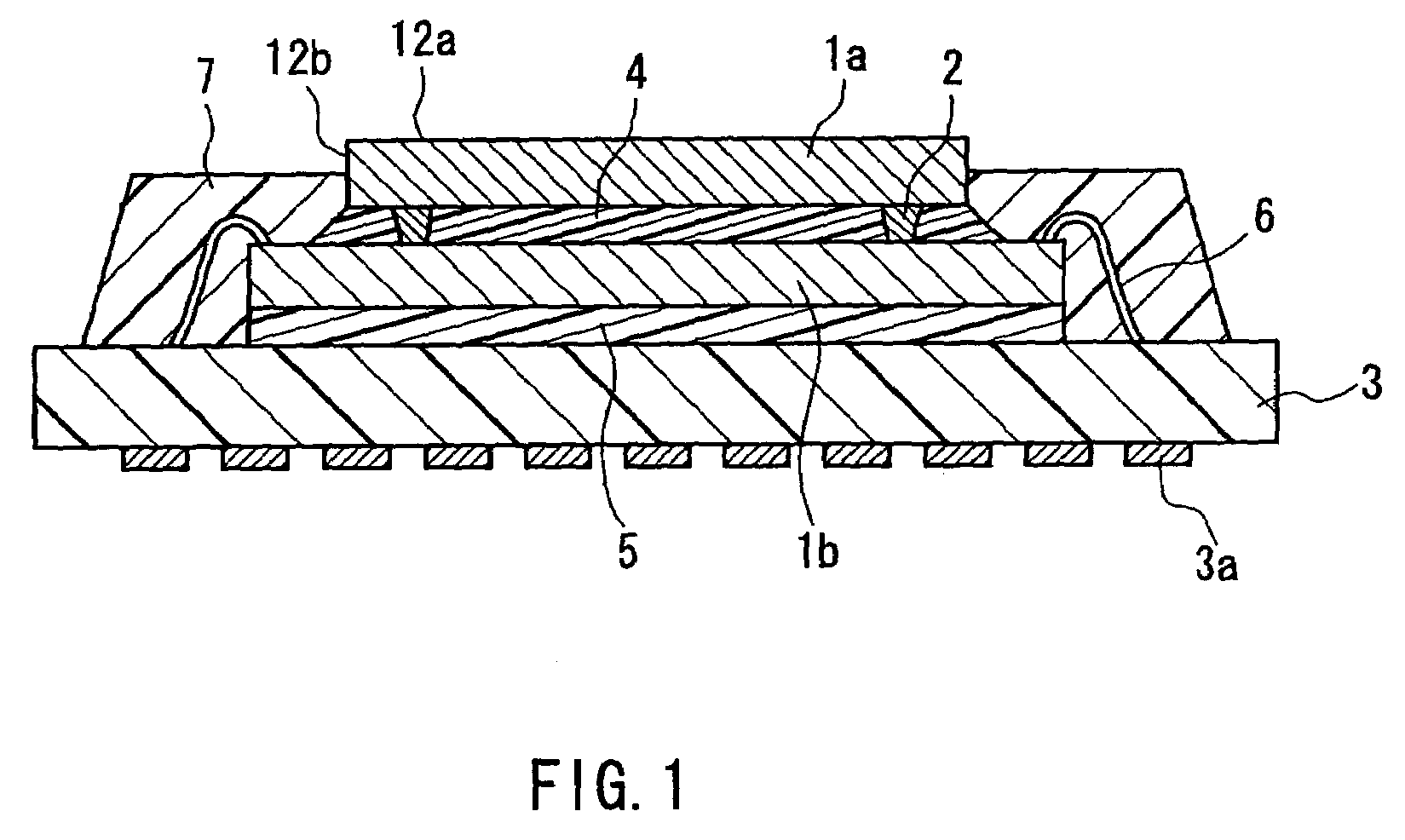
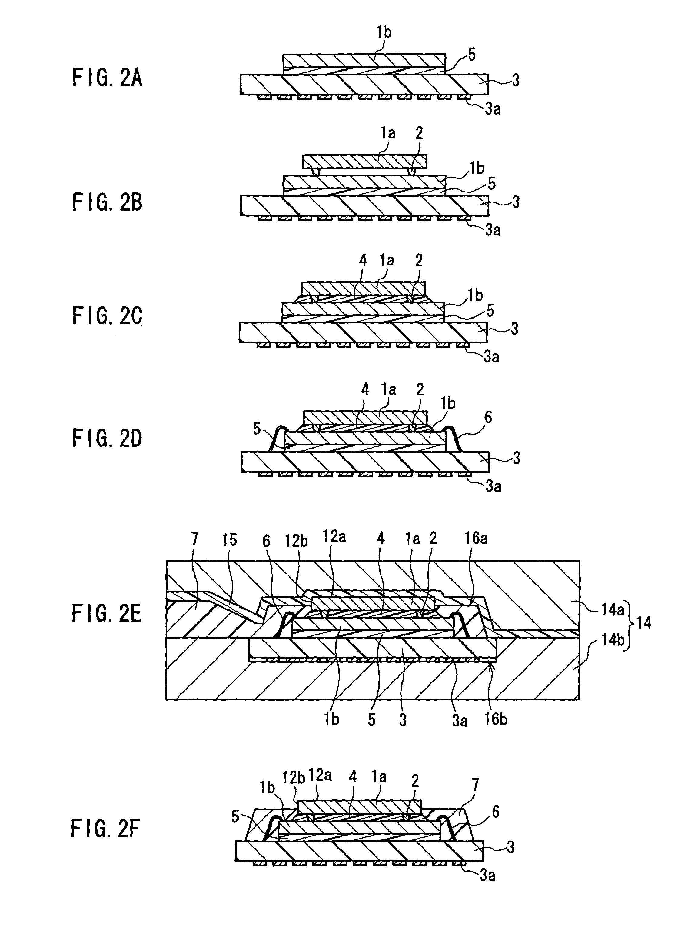
[0054]A semiconductor device and a method for manufacturing the same according to Embodiment 1 will be described below with reference to FIGS. 1 and 2A to 2F. First, a semiconductor device according to Embodiment 1 will be described with reference to FIG. 1. FIG. 1 is a cross-sectional view showing a configuration of a semiconductor device according to Embodiment 1 of the present invention.

[0055]As shown in FIG. 1, similar to the conventional semiconductor device described above with reference to FIG. 9, the semiconductor device according to Embodiment 1 includes a substrate 3, a first semiconductor chip 1a and second semiconductor chip 1b mounted on the substrate 3 by stacking the first semiconductor chip 1a on the second semiconductor chip 1b, and an encapsulation resin layer 7 formed of encapsulation resin.

[0056]The first semiconductor chip 1a as the uppermost semiconductor chip is mounted on the substrate 3 with the circuit surface thereof facing toward the substra...

embodiment 2

(Embodiment 2)

[0093]A semiconductor device and a method for manufacturing the same according to Embodiment 2 will be described below with reference to FIGS. 3 and 4A to 4E. First, a semiconductor device according to Embodiment 2 will be described with reference to FIG. 3. FIG. 3 is a cross-sectional view showing a configuration of a semiconductor device according to Embodiment 2 of the present invention.

[0094]As shown in FIG. 3, the semiconductor device according to Embodiment 2 differs from the semiconductor device according to Embodiment 1 in that: (1) a portion of a first semiconductor chip 1a is fixed to a portion of a second semiconductor chip 1b with an adhesive 8; and (2) instead of the underfill material 4 (see FIG. 1), encapsulation resin for forming an encapsulation resin layer 7 is transferred into a space formed between the first semiconductor chip 1a and the second semiconductor chip 1b by bumps 2.

[0095]Except for these two points, the semiconductor device according to ...

embodiment 3

(Embodiment 3)

[0121]A semiconductor device and a method for manufacturing the same according to Embodiment 3 will be described below with reference to FIGS. 5 and 6A to 6E. First, a semiconductor device according to Embodiment 3 will be described with reference to FIG. 5. FIG. 5 is a cross-sectional view showing a configuration of a semiconductor device according to Embodiment 3 of the present invention.

[0122]As shown in FIG. 5, the semiconductor device according to Embodiment 3 differs from the semiconductor device according to Embodiment 2 in that a lead frame 9 is used as a substrate on which a first semiconductor chip 1a and a second semiconductor chip 1b are mounted.

[0123]Furthermore, as shown in FIG. 5, the lead frame 9 includes a die pad portion 9a on which a second semiconductor chip 1b is mounted, an inner lead portion 9b to which wires 6 are connected, and a land portion 9c to which an external component or device is connected. Examples of the material for forming the lead...


PUM


Abstract

A semiconductor device with excellent heat dissipation characteristics that can achieve a high reliability when mounted in electronic equipment such as a cellular phone or the like and a method for manufacturing the same are provided. The semiconductor device includes a substrate, a plurality of semiconductor chips mounted on the substrate by stacking one on top of another, and an encapsulation resin layer made of encapsulation resin. Among the plurality of semiconductor chips, a first semiconductor chip as an uppermost semiconductor chip is mounted with a surface thereof on which a circuit is formed facing toward the substrate, and the encapsulation resin layer is formed so that at least a surface of the first semiconductor chip opposite to the surface on which the circuit is formed and a part of side surfaces of the first semiconductor chip are exposed to the outside of the encapsulation resin layer.

Description

BACKGROUND OF THE INVENTION[0001]1. Field of the Invention[0002]The present invention relates generally to a semiconductor device and a method for manufacturing the same.[0003]2. Description of the Related Art[0004]In methods for manufacturing a semiconductor device by using a plurality of semiconductor chips with different functions, the semiconductor device is manufactured by cutting out the semiconductor chips with different functions from a plurality of wafers obtained through different processes and using them in any desired combinations. Thus, in general, these methods are superior to methods for manufacturing a semiconductor device by integrating all the desired functions onto one chip in terms of manufacturing cost.[0005]One of the above-described methods for manufacturing a semiconductor device by using a plurality of semiconductor chips with different functions is called a “chip-on-chip method”, in which a plurality of semiconductor chips are stacked vertically and connect...

Claims


Application Information

Patent Timeline
IPC IPC(8): H01L21/44H01L23/28H01L21/56H01L23/12H01L25/065H01L25/07H01L25/18
CPCH01L21/565H01L25/0657H01L2224/92125H01L2224/16145H01L2224/16225H01L2224/48091H01L2224/48225H01L2224/48227H01L2224/731H01L2224/73207H01L2224/73265H01L2225/0651H01L2225/06517H01L2225/06558H01L2225/06568H01L2225/06582H01L2225/06589H01L2924/01046H01L2924/01078H01L2924/01079H01L2924/18161H01L25/0652H01L2924/1815H01L2224/32145H01L2224/32225H01L2224/32245H01L2224/73204H01L2924/01019H01L2924/10253H01L2924/00014H01L2924/00H01L2224/0401
Inventor ARAI, YOSHIYUKIYUI, TAKASHITAKEOKA, YOSHIAKIITOU, FUMITOYAMAUCHI, KOUICHIYAGUCHI, YASUTAKE
Owner TESSERA ADVANCED TECH
Why Eureka
Try Eureka