Electron emission device and electron emission display having beam-focusing structure using insulating layer

a technology of electron emission display and electron emission device, which is applied in the direction of discharge tube luminescnet screen, discharge tube main electrode, instruments, etc., can solve the problems of lowering a yield, complicated fabrication process, and difficult fabrication process of conventional electron emission device, and achieves simple fabrication process and excellent focusing of electron beam

Inactive Publication Date: 2006-11-21
SAMSUNG SDI CO LTD
View PDF8 Cites 5 Cited by
  • Summary
  • Abstract
  • Description
  • Claims
  • Application Information

AI Technical Summary

Benefits of technology

[0019]Accordingly, it is an aspect of the present invention to provide an electron emission device and an electron emission display having a beam-focusing structure using an insulating layer, which is not only excellent in focusing an electron beam but also has a simple fabricating process.
[0020]Another aspect of the present invention is to provide an electron emission device and an electron emission display using the same in which the electron emission device is fabricated by a simple, low-cost process, and is improved in focusing efficiency.

Problems solved by technology

Because of this, the fabricating process for the conventional electron emission device is difficult.
Such conventional electron emission device with the vertical focusing electrode is excellent in focusing the electron beam, but has a complicated fabricating process because the insulator formed on the gate electrode should be thick with a thickness of a few μm to a few hundreds μm, thereby lowering a yield thereof.

Method used


Image

  • Electron emission device and electron emission display having beam-focusing structure using insulating layer
  • Electron emission device and electron emission display having beam-focusing structure using insulating layer
  • Electron emission device and electron emission display having beam-focusing structure using insulating layer

Examples


Embodiment Construction

[0038]In the following detailed description, exemplary embodiments of the present invention are shown and described by way of illustration. Accordingly, the drawings and description are to be regarded as illustrative in nature, and not restrictive.

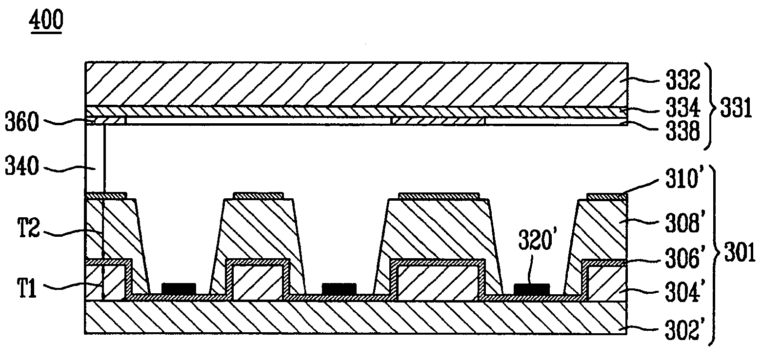
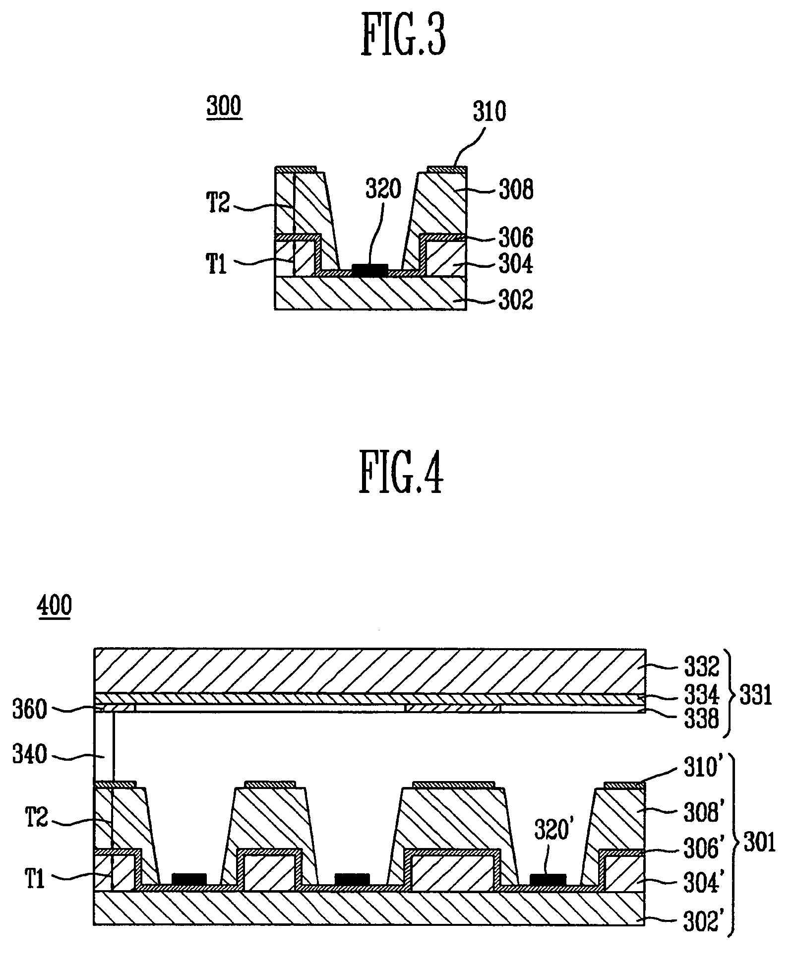
[0039]FIG. 3 is a sectional view of an electron emission device having a beam-focusing structure according to an embodiment of the present invention.

[0040]Referring to FIG. 3, an electron emission device 300 includes a plate 302, a first insulating layer 304, a cathode electrode 306, a second insulating layer 308, a gate electrode 310, and an electron emission portion 320. The plate 302 may be formed of a transparent plate such as a vitreous plate.

[0041]The first insulating layer 304 is made of insulating material having a first etching rate and formed on the plate 302. The first insulating layer 304 is formed with a first hole through which the plate 302 or a buffer layer (not shown) on the plate 302, to be formed with the electron emissi...


PUM


Abstract

An electron emission device and / or display using the same includes a beam-focusing structure. The beam-focusing structure has a first insulating layer formed on a plate. The first insulating layer has a thickness, and is formed with a first hole. A first electrode is formed on the first insulating layer and extending into the first hole. An emission portion is formed in the first hole and connected to the first electrode. A second insulating layer is formed on the first electrode and is also formed with a second hole through which the emission portion is at least partially exposed. A second electrode is formed on the second insulating layer. In the electron emission device and / or the display, an electric field between the first electrode and the second electrode causes the emission portion to emit an electron beam and focuses the electron beam from the emission portion.

Description

CROSS-REFERENCE TO RELATED APPLICATIONS[0001]This application claims priority to and the benefit of Korean Patent Application No. 10-2004-0037549, filed May 25, 2004 in the Korean Intellectual Property Office, the entire content of which is incorporated herein by reference.BACKGROUND[0002]1. Field of the Invention[0003]The present invention relates to an electron emission device, and more particularly, to an electron emission device and an electron emission display having a beam-focusing structure using an insulating layer.[0004]2. Discussion of Related Art[0005]Generally, an electron emission device can be classified into a hot cathode-type and a cold cathode-type. The hot cathode-type and the cold cathode-type employ a hot cathode and a cold cathode as an electron emission portion, respectively.[0006]Also, a cold cathode-type electron emission device can have a structure such as a field emitter array (FEA), a surface conduction emitter (SCE), a metal insulator metal (MIM), a metal...

Claims


Application Information

Patent Timeline
Patent Type & Authority Patents(United States)
IPC IPC(8): H01J1/304H01J29/50H01J1/30
CPCH01J3/022H01J2201/30407H01J2329/00G07F19/205G07F19/201G07D2211/00
Inventor KIM, SI MYEONG
Owner SAMSUNG SDI CO LTD
Why Eureka
Try Eureka