
Display device and driving method thereof

a technology of display device and driving method, which is applied in the direction of static indicating device, electroluminescent light source, instruments, etc., can solve the problems of fluctuation of actual current flow, fluctuation of /b>, and current flowing in the oled, so as to reduce size, reduce cost, and high cost

Inactive Publication Date: 2006-11-21
SEMICON ENERGY LAB CO LTD
View PDF65 Cites 97 Cited by
  • Summary
  • Abstract
  • Description
  • Claims
  • Application Information

AI Technical Summary

Benefits of technology

The present invention is a display device that includes a pixel with a current supply circuit, a switch portion, and a light emitting element. The device uses a digital video signal to control the light emitting element and can display in gray scales. The device also includes means for preventing the second current from flowing into the light emitting element using a different signal than the digital video signal. The ratio of the current can be changed to display in gray scales, and the device can display in non-display periods. The technical effects of the invention include improved image quality, reduced power consumption, and improved control of brightness and gray scales.

Problems solved by technology

The voltage writing type analog method described above has a problem in that the current flowing in the OLED 3006 fluctuates greatly due to changes in drain current caused by fluctuation in current characteristic of the driving TFT 3004 when signals inputted to pixels from their respective source signal lines 3003 have the same electric potential.
Therefore a problem of conventional display devices in which driving TFTs operate in a linear range, typically, voltage writing type digital method display devices, is that the amount of current actually flows is varied even when a constant voltage is applied between two electrodes of an OLED.
Therefore it is difficult to write a signal current quickly.
However, in practice, matching the current characteristics of the TFTs that forms a pair exactly is difficult and it results in fluctuation.
This brings a problem of reduction in contrast.
For that reason, it is difficult to manufacture video signal input current supplies having the same current characteristic in transistors that use a polycrystalline semiconductor thin film.
Bonding the chip requires a large area, which is a problem because it makes reduction of the frame area in the periphery of the pixel region impossible.

Method used


Image

  • Display device and driving method thereof
  • Display device and driving method thereof
  • Display device and driving method thereof

Examples


embodiment mode 1

[0183]An example of the pixel structure is shown for a display device of the present invention. FIG. 4 shows a structural example of a current supply circuit placed in each pixel. In FIG. 4, components identical with those in FIG. 3 are denoted by the same symbols. The example shown in FIG. 4 is of a current mirror method current supply circuit. A current supply circuit 102 is composed of a current supply capacitor 111, a current supply transistor 112, a current transistor 1405, a current input transistor 1403, a current holding transistor 1404, a current line CL, a signal line GN, and a signal line GH. The current supply transistor 112 and the current transistor 1405 form a pair to constitute a current mirror circuit, and therefore have to have the same polarity. Desirably, these two transistors in the same pixel have the same current characteristic. In Embodiment Mode 1, the current characteristic of the current supply transistor 112 and the current characteristic of the current t...

embodiment mode 2

[Embodiment Mode 2]

[0293]This embodiment mode shows a structural example of an identic-transistor method current supply circuit with reference to FIG. 12. The description here is mainly about a difference between this embodiment mode and Embodiment Mode 1 and explanations for things that overlap will be omitted. Accordingly, components in FIG. 12 that are identical with those in FIG. 3 are denoted by the same symbols.

[0294]In FIG. 12, a current supply circuit 102 is composed of a current supply capacitor 111, a current supply transistor 112, a current input transistor 203, a current holding transistor 204, a current stopping transistor 205, a current line CL, a signal line GN, a signal line GH, and a signal line GS. The current supply transistor 112 is a p-channel transistor in the example shown. If an n-channel transistor is used for the current supply transistor 112, follow the structure shown in FIG. 3(C) for easy application. An example thereof is shown in FIG. 24. Components id...

embodiment mode 3

[Embodiment Mode 3]

[0331]This embodiment mode describes a multi-gate method current supply circuit. The description here is mainly about a difference between this embodiment mode and Embodiment Modes 1 and 2, and explanations for things that are common will be omitted.

[0332]The structure of a current supply circuit using a multi-gate method 1 is described with reference to FIG. 57. Components identical with those in FIG. 3 are denoted by the same symbols. The current supply circuit of multi-gate method 1 has a current supply transistor 112 and a current stopping transistor 805. The circuit also has a current input transistor 803 and current holding transistor 804 that function as switches. The current supply transistor 112 can either be a p-channel transistor or an n-channel transistor and the same applies to the current stopping transistor 805, the current input transistor 803, and the current holding transistor 804. However, the current supply transistor 112 and the current stoppi...


PUM


Abstract

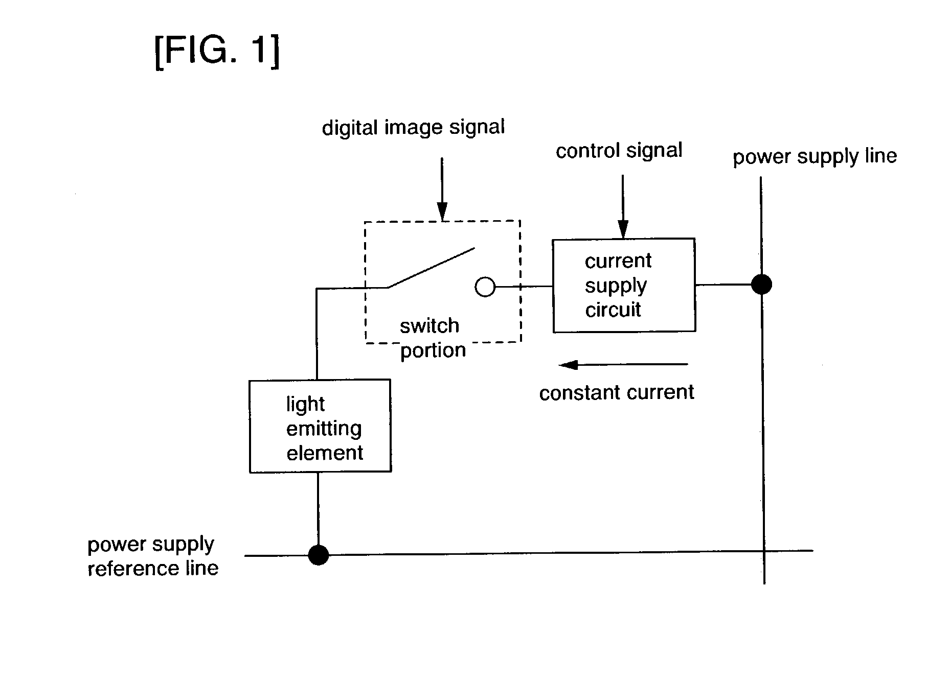
Each pixel of a display device has a current supply circuit, a switch portion, and a light emitting element. The light emitting element, the current supply circuit, and the switch portion are connected in series between a power supply reference line and a power supply line. The switch portion is switched between ON and OFF using a digital video signal. The amount of constant current flowing in the current supply circuit is determined by a control signal inputted from the outside of the pixel. When the switch portion is ON, a constant current determined by the current supply circuit flows in the light emitting element and light is emitted. As a result, a low-cost display device can be provided in which the light emitting element can emit light at a constant luminance even when the current characteristic is changed by degradation or the like, which is fast in writing signals in pixels, which can display in gray scales accurately, and which can be reduced in size with a low cost, as well as a driving method of the display device.

Description

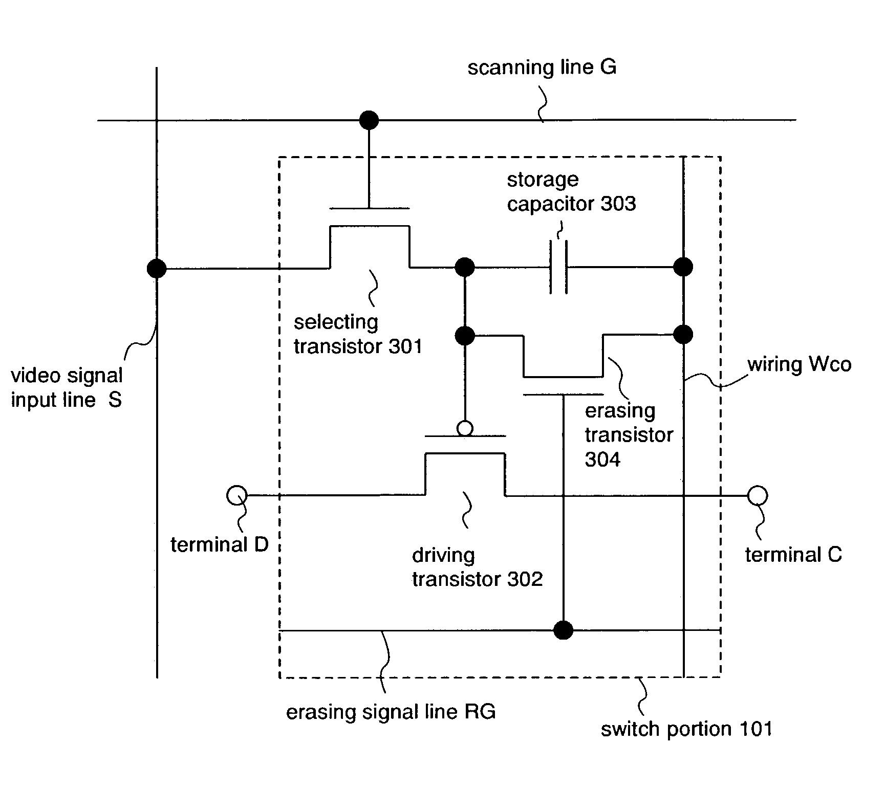
TECHNICAL FIELD[0001]The present invention relates to a display device and a driving method thereof. Specifically, the invention relates to an active matrix display device in which a transistor is provided in each pixel to control light emission of the pixel, and to a method of driving the display device.BACKGROUND ART[0002]An active matrix display device has been proposed in which each pixel has a light emitting element and a transistor for controlling light emission of the light emitting element. A light emitting element refers to an element which has a first electrode and a second electrode and whose luminance is controlled by the amount of current flowing between the first electrode and the second electrode. Display devices using OLED (Organic Light Emitting Diode) elements as light emitting elements (hereinafter referred to as OLED display devices) are attracting attention. OLED display devices have advantages such as excellent responsiveness, low voltage operation, and wide vi...

Claims


Application Information

Patent Timeline
Patent Type & Authority Patents(United States)
IPC IPC(8): G09G3/10G09G3/30G09G3/36G09G3/20G09G3/32G09G5/00G09G5/399H05B44/00
CPCG09G3/3241G09G3/3266G09G3/3283G09G5/399G09G5/008G09G3/2022G09G2360/18G09G2300/0842G09G2300/0861G09G3/3225G09G3/30
Inventor KIMURA, HAJIME
Owner SEMICON ENERGY LAB CO LTD
Learn More