Apparatus and method for growth of a thin film

a thin film and apparatus technology, applied in the direction of crystal growth process, polycrystalline material growth, chemically reactive gas growth, etc., to achieve the effect of reducing undesirable reactions

Inactive Publication Date: 2006-11-28
ASM IP HLDG BV
View PDF39 Cites 202 Cited by
  • Summary
  • Abstract
  • Description
  • Claims
  • Application Information

AI Technical Summary

Benefits of technology

[0010]The present invention provides an improved apparatus and method for substrate layer deposition in which substrate layers are grown by carrier gas delivery of sequential pulses of reactants to the substrate surface. At least one of the reactants comprises excited species, e.g., radicals. In a specific embodiment, the apparatus of this invention provides sequential repeated pulses of reactants in a flow of carrier gas for reaction at a substrate surface. The reactant pulses are delivered with sufficient intervening delay times to minimize undesirable reaction between reactants in adjacent pulses in the gas phase or undesired uncontrolled reactions on the substrate surface. We have found that depending on reactor design, there is a pressure range where sufficient excited species, including radicals, survive and where an inert gas phase diffusion barrier can be used.
[0012]The use of reactant pulses separated in time and space in a carrier gas flow significantly increases the speed of processing because intervening chamber pump down steps are not required. Use of the methods and apparatus of this invention results in high layer growth rates typically greater than about 1–10 nm / min.

Problems solved by technology

However, remote radical generation techniques should provide sufficient radical densities at the substrate surface, notwithstanding the significant losses that can occur on transport of the radical to the reaction chamber.

Method used


Image

  • Apparatus and method for growth of a thin film
  • Apparatus and method for growth of a thin film
  • Apparatus and method for growth of a thin film

Examples


Embodiment Construction

[0017]The invention is further described by reference to the figures in which the same numbers indicate like features.

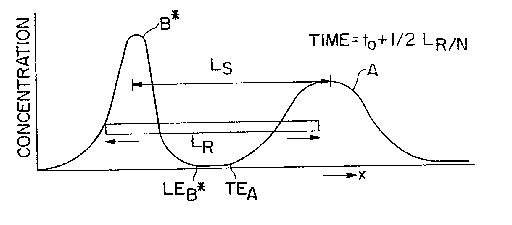
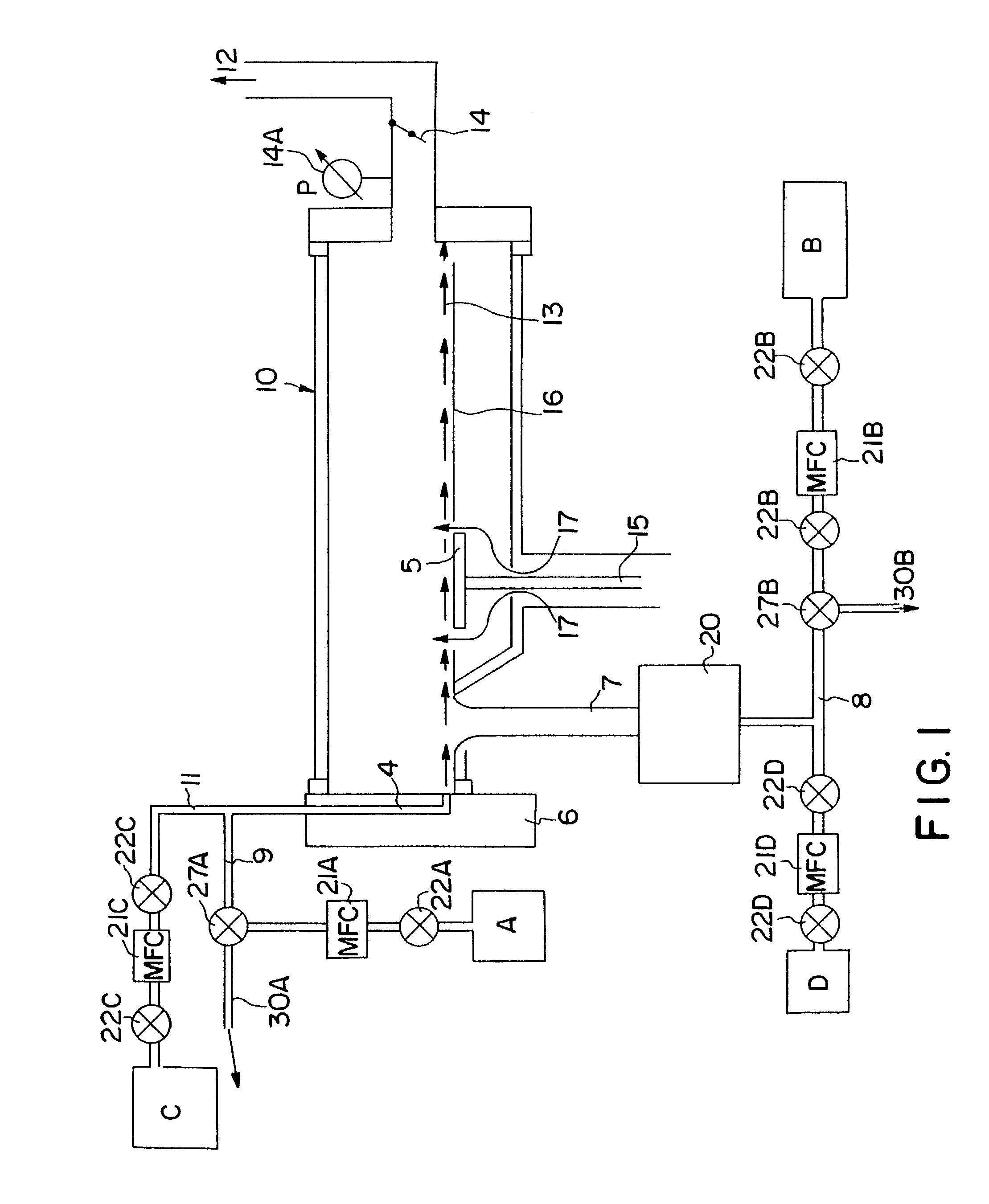
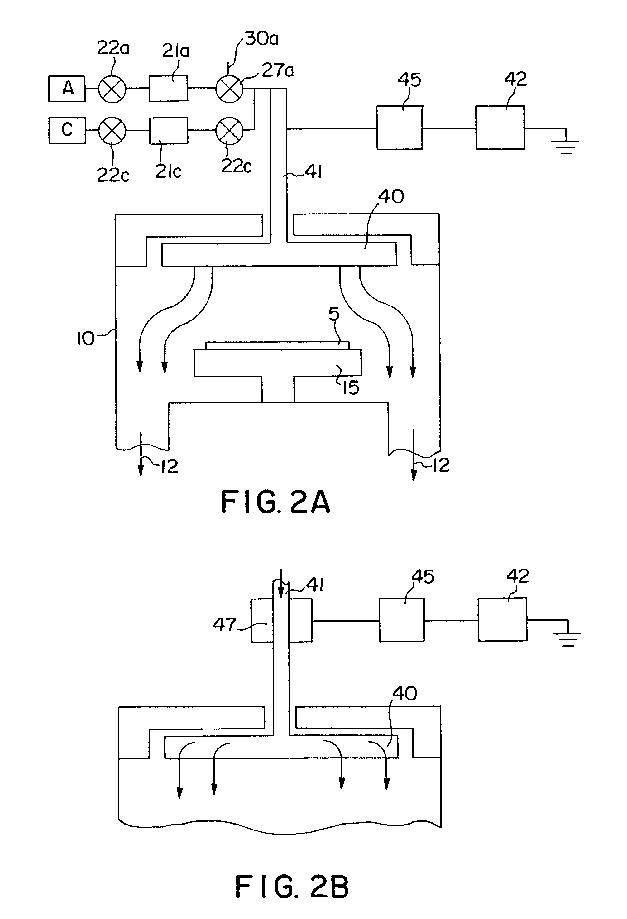
[0018]FIG. 1 illustrates a deposition apparatus of this invention adapted for delivery of sequential pulses of two different reactants A and B*, one of which B* contains excited species, to a substrate. The apparatus has a reaction chamber 10 with substrate 5 positioned on holder 15 which is optionally heated. The substrate holder can be heated resistively, inductively or by use of infrared lamps, as is known in the art. Gases flow into the reactor through one or more gas inlets 4 at the injector flange 6. Residual gases, after passage over the substrate are removed through an exhaust conduit 12 provided with a throttle valve 14 and a pressure measurement and control 14A. The reactor chamber illustrated is a radiantly heated, horizontal flow cold wall reactor, typically made of quartz, and having a divider plate 16 substantially aligned with the top surface of the su...


PUM

PropertyMeasurementUnit
pressuresaaaaaaaaaa
pressureaaaaaaaaaa
diameter×5aaaaaaaaaa

Abstract

An improved apparatus and method for substrate layer deposition in which substrate layers are grown by carrier gas delivery of sequential pulses of reactants to the substrate surface. At least one of the reactants comprises excited species, e.g., radicals. In a specific embodiment, the apparatus of this invention provides sequential repeated pulses of reactants in a flow of carrier gas for reaction at a substrate surface. The reactant pulses are delivered with sufficient intervening delay times to minimize undesirable reaction between reactants in adjacent pulses in the gas phase or undesired uncontrolled reactions on the substrate surface.

Description

REFERENCE TO RELATED APPLICATIONS [0001]This application is a Continuation of U.S. Ser. No. 09,392,371 filed Sep. 8, 1999 now U.S. Pat. No. 6,511,539.BACKGROUND OF THE INVENTION[0002]This invention relates generally to improved apparatus and methods for deposition processes in the manufacture of semiconductor materials.[0003]Chemical vapor deposition (CVD) processes have long been used to form thin layers on substrates (and wafers) by sequential layer deposition by thermal reaction or decomposition of gaseous material (reactants) at the substrate surface. In a specific type of deposition process, atomic layer epitaxy (ALE), sequential monolayers are deposited on a substrate surface by alternate exposure to chemical reactants. Repeated exposure cycles of the substrate to reactant gases builds the desired layer structure. ALE techniques are described for example in M. Ritala et al. (1998) J. ElectroChemical Society 145:2914; H. Shrinriki et al. (1998) J. ElectroChemical Society 145:32...

Claims


Application Information

Patent Timeline
Patent Type & Authority Patents(United States)
IPC IPC(8): H01L21/44C23C16/04C30B25/12H05H1/00C23C16/44C23C16/452C23C16/455H01L21/205
CPCC23C16/452C23C16/45521C23C16/45536C23C16/45542C30B25/14C30B29/38H01J37/3244C23C16/45544Y10T117/10H01L21/205
Inventor RAAIJMAKERS, IVO
Owner ASM IP HLDG BV
Why Eureka
Try Eureka