Apparatus for micro-electro mechanical system package

a micro-electromechanical and apparatus technology, applied in electrical apparatus, semiconductor devices, semiconductor/solid-state device details, etc., can solve the problems of unsuitable packages for this application, and unsuitable packages for many mems applications, etc., to achieve convenient use and higher device yields

Active Publication Date: 2006-11-28
MIRADIA INC
View PDF3 Cites 16 Cited by
  • Summary
  • Abstract
  • Description
  • Claims
  • Application Information

AI Technical Summary

Benefits of technology

[0012]Many benefits are achieved by way of the present invention over conventional techniques. For example, the present technique provides an easy to use process that relies upon conventional technology. In some embodiments, the method provides higher device yields. Additionally, the method provides a process that is compatible with conventional process technology without substantial modifications to conventional equipment and processes. Depending upon the embodiment, one or more of these benefits may be achieved. These and other benefits will be described in more throughout the present specification and more particularly below.

Problems solved by technology

The package illustrated in FIG. 1 presents several drawbacks in applications that often require more than electrical operation of the silicon integrated circuit.
The optical properties of the plastic encapsulant, including lack of transparency, non-uniformity of the index of refraction, and surface roughness make these packages unsuitable for this application.
The physical contact that the plastic encapsulant makes with the surface of the integrated circuit, therefore, make this package unsuitable for many MEMS applications.
Despite progress in packaging MEMS in hermetically sealed packages, there are still limitations.
For example, the conventional MEMS package is often expensive and difficult to manufacture.
Additionally, the conventional MEMS package often requires a certain amount of chip real estate, which is expensive and leads to larger package designs.

Method used


Image

  • Apparatus for micro-electro mechanical system package
  • Apparatus for micro-electro mechanical system package
  • Apparatus for micro-electro mechanical system package

Examples


Embodiment Construction

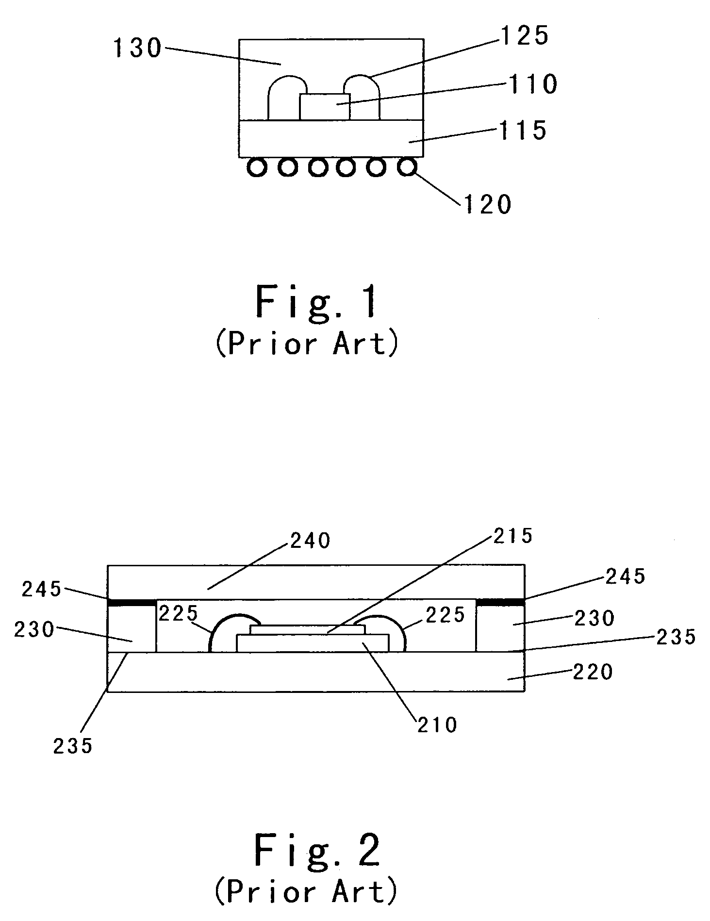
[0024]This present invention relates generally to manufacturing objects. More particularly, the invention provides a method and apparatus for packaging a MEMS. Merely by way of example, the invention has been applied to a MEMS with a transparent glass cover bonded to a ball grid array with a reduced lateral separation between the transparent glass cover and the ball grid array. The method and apparatus can be applied to display technology as well as, for example, charge coupled display camera arrays, and infrared arrays.

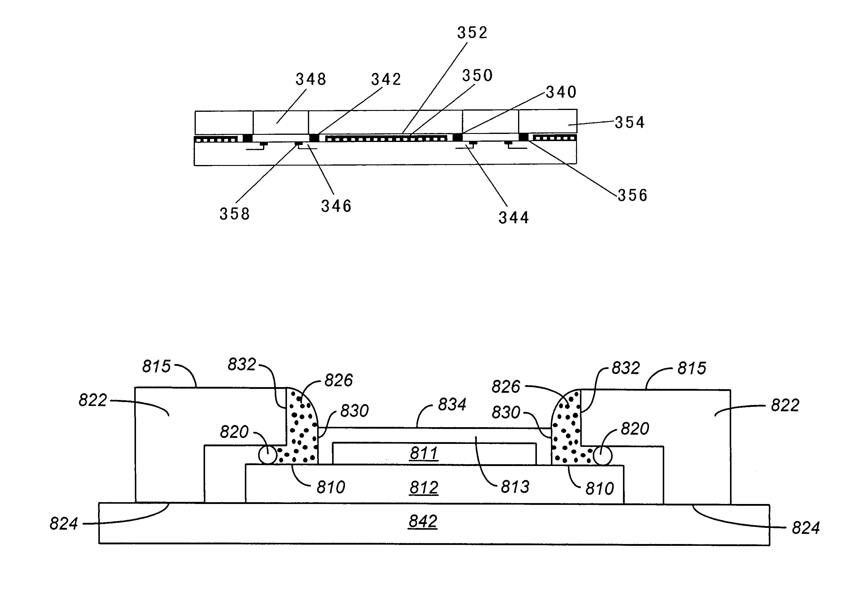
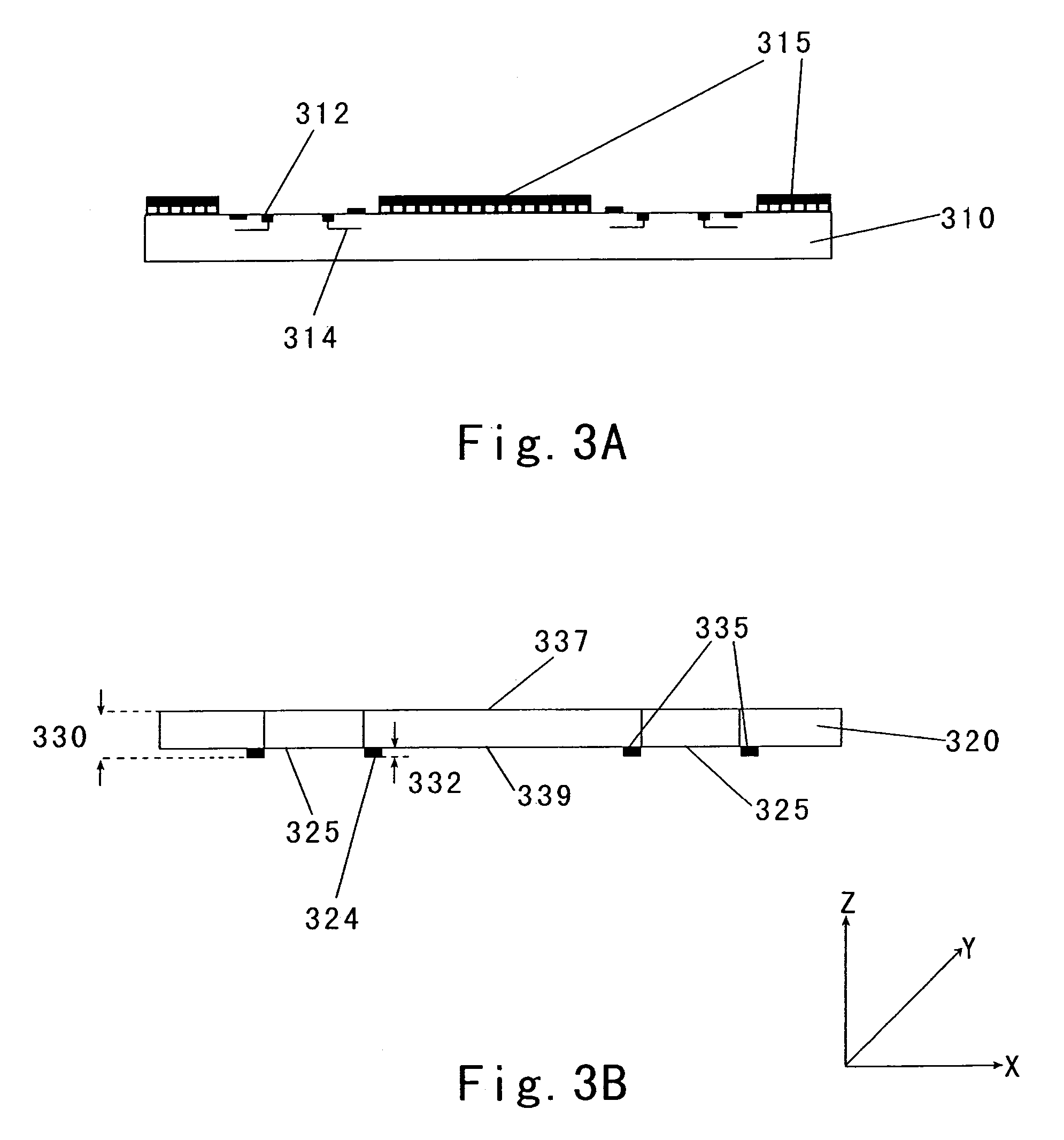
[0025]FIGS. 3A–3D are simplified diagrams of a wafer-level hermetically sealed package according to embodiments of the present invention. These diagrams illustrate examples according to specific embodiments. One of ordinary skill in the art would recognize various modifications, alternatives and variations. Preferably, formation of the package occurs prior to separation of the active devices into die form. Here, separation often occurs using a dicing and / or scribing ...


PUM


Abstract

A method of manufacturing a multi-substrate semiconductor package. The method includes providing a first substrate with a plurality of first dies present thereon and forming a plurality of electrical contacts on an upper surface of a lateral extension portion of at least one of the plurality of first dies on the first substrate. The method also includes providing a second substrate, the second substrate comprising a plurality of second dies, at least one of the plurality of second dies comprising an interconnect region. Further, the method includes forming a sandwich structure by bonding the second substrate to an upper surface of the first substrate to form an intermediate level within the sandwich structure and separating the dies. The method also includes coupling an electrically conductive structure through the interconnect region of the one second dies to the lateral extension portion of the one first die.

Description

BACKGROUND OF THE INVENTION[0001]This present invention relates generally to manufacturing objects. More particularly, the invention provides a method and apparatus for packaging a micro-electromechanical system (MEMS). Merely by way of example, the invention has been applied to a MEMS with a transparent glass cover bonded to a ball grid array with a reduced lateral separation between the transparent glass cover and the ball grid array. The method and apparatus can be applied to display technology as well as, for example, charge coupled display camera arrays, and infrared arrays.[0002]The packaging of silicon integrated circuits has reached a high level of maturity. FIG. 1 illustrates a simplified diagram of a conventional silicon integrated circuit package. The silicon integrated circuit die 110 is mounted on a submount 115 featuring a ball grid array 120. Wire bonds 125 are attached to the silicon die 110 to provide electrical connection to the submount 115. Typically, the silicon...

Claims


Application Information

Patent Timeline
Patent Type & Authority Patents(United States)
IPC IPC(8): H01L23/495H01L21/30
CPCB81B7/0067H01L2224/48227H01L2924/01079H01L2924/16235H01L2924/01322H01L2224/45144H01L2924/00H01L2924/10253H01L2924/16195
Inventor YANG, XIAO
Owner MIRADIA INC
Why Eureka
Try Eureka