Driving device and image display apparatus

Inactive Publication Date: 2006-11-28
CANON KK
View PDF32 Cites 0 Cited by
  • Summary
  • Abstract
  • Description
  • Claims
  • Application Information

AI Technical Summary

Benefits of technology

[0030]The present invention has been made in view of the above technical background and a primary object of this invention is to provide a driving device capable of accurately driving image display elements in accordance with inputted luminance data. Another object of the invention is to provide an image display apparatus capable of displaying high fidelity images with enhanced picture quality.

Problems solved by technology

Unfortunately, currently available large-screen high-definition image display apparatus with enhanced fidelity and increased resolution capability—such as displays with 1,920 by 1,080 dots of effective pixels and a frame rate of 60 hertz (Hz) and also 10-bit gradation tonality—are encountered with problems which follow.
However, in view of electrical characteristics of components making up drive circuitry such as integrated circuit (IC) chips and printed wiring boards and power supply units, it remains difficult to achieve such level of resolution.
This wave edge rounding would result in a decrease in display quality at low luminance levels.
In other words, it is no longer achievable to visually display any image with desired tonality in low gradation regions.
Also note that in the case of supplying constant current pulses with short time lengths from a control constant current source to a multi-electron source unit with a very large number of matrix-wired electron emitting elements, a problem that electrons are hardly released in any way arises.
Obviously, electrons are emitted in case constant current pulses are continuously supplied within a relatively long time period; however, a lengthened rise-up time must be required until initiation of electron emission.
Such waveform rounding results in deformation or distortion of the waveform of an emission current Ie.
Additionally the voltage drive schemes are faced with problems to be solved as follows.
Furthermore, owing to the self-inductive action of the parasitic inductance, an electromotive force of U=−L×(di / dt) is produced resulting in generation of over-shooting and / or ringing, which leads to unwanted occurrence of application of abnormal voltages to light emitting elements.
The quest for larger screen sizes and higher precision and higher tonality results in increases in parasitic inductance and capacitance of electrical wires used.
Hence, the problems such as the failure of tonality in dark regions due to the rounding of rising edge of the drive waveform, the overshoot and the ringing are becoming more serious issues to be solved.
Another problem of the approach using drive waveforms created by means of plain pulse width control and pulse peak value control schemes is that uniform increasing characteristic of the grayscale / gradation tonality is no longer guaranteeable due to any possible changes and fluctuations of the voltage versus luminescence intensity characteristics of light emitting elements.
With such aligned pulses, a large current rushes to flow in a scan wiring at the time of potential rise-up of a pulse width modulation waveform, resulting in occurrence of a voltage drop.
A result of this is that the emission electron distribution pattern of each element fails to stay uniform.
And,when applying such multi-electron source unit to image display apparatus, a problem arises that the display quality can decrease due to the voltage drop as created by the wiring resistance.
However, such voltage difference is no longer negligible in some cases—for example, when the row wiring has an increased value of resistance due to an increase in screen size of image display apparatus.
The voltage difference also becomes greater in cases where the pixels used increase in number resulting in an increase in current flowing into the row wiring.

Method used


Image

  • Driving device and image display apparatus
  • Driving device and image display apparatus
  • Driving device and image display apparatus

Examples


first embodiment

(First Embodiment)

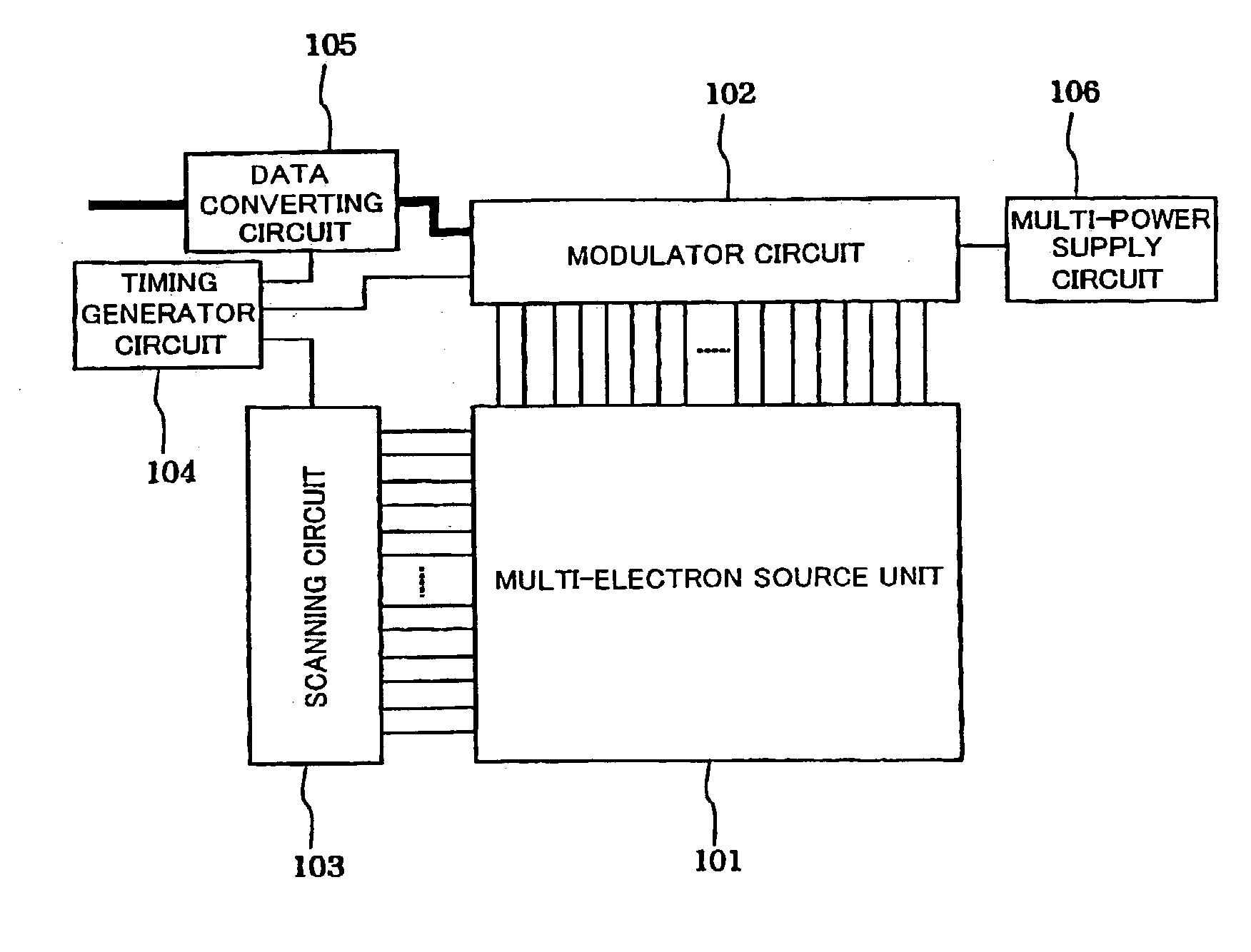
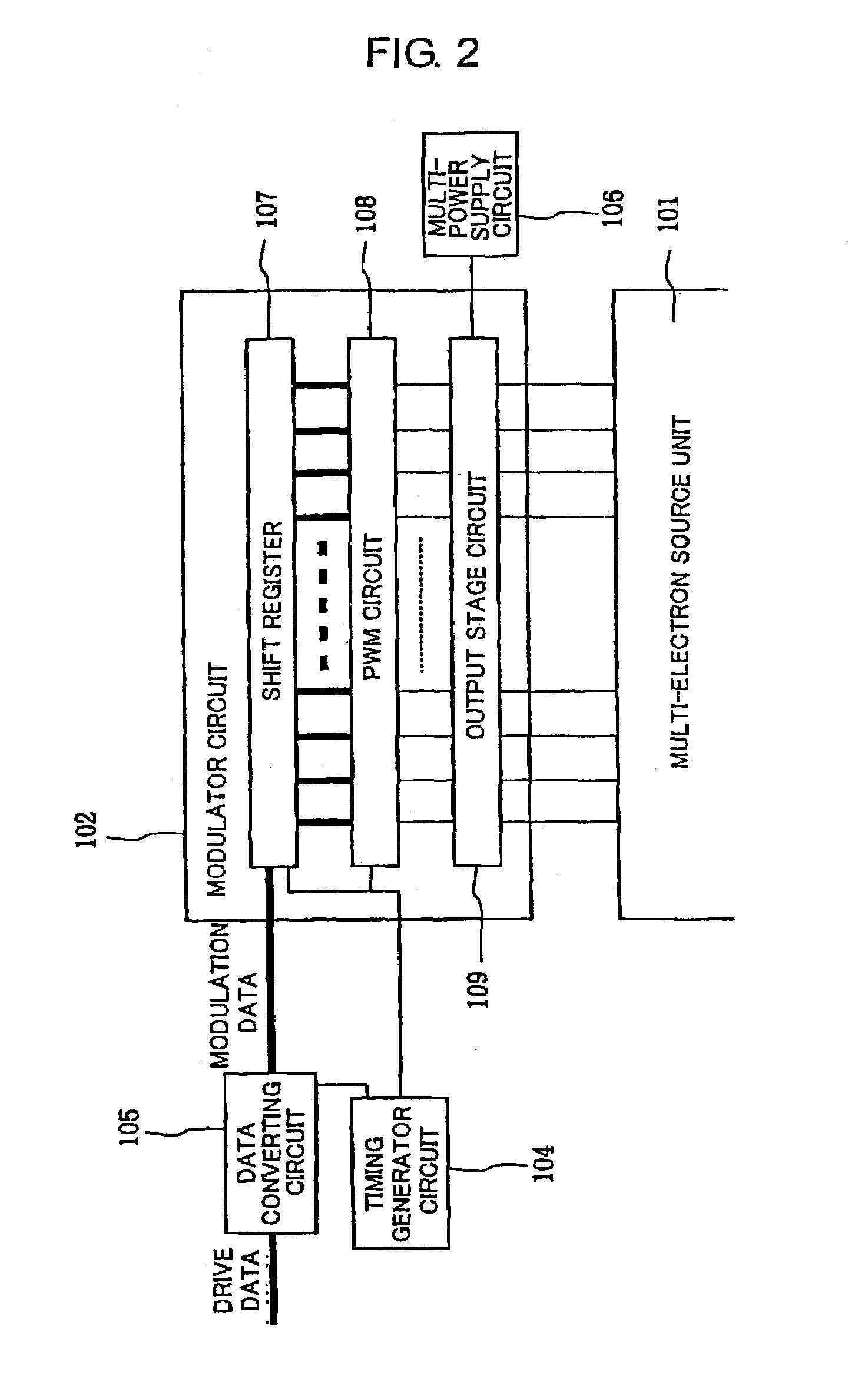
[0065]FIG. 1 illustrates, in schematic block diagram form, a driving device in accordance with a first embodiment of the invention. As shown herein, the driving device is arranged to have a modulator circuit (modulation means) 102, a scanning circuit (selection means) 103, a timing generator circuit 104, a data converting circuit 105, and a multiple-power supply circuit 106. This driving device is a circuit for driving a multiple-electron source unit 101, which makes up an image display module of image display apparatus.

[0066]The multi-electron source unit 101 is the one with electron sources (image display elements) 1 being disposed at cross points of row wirings 2 and column wirings 3 as shown in FIG. 28.

[0067]The electron sources may preferably be cold cathode elements. These cold cathode elements are capable of obtaining the intended electron emission at low temperatures when compared to hot cathode elements and, therefore, do not require any extra heaters for ...

second embodiment

(Second Embodiment)

[0125]A second embodiment of the invention will be described with reference to FIGS. 24 to 26 below. Although in the first embodiment stated above is arranged to employ the same dispersion rule to all the column wirings involved, the second embodiment is such that the dispersion rule to be applied to one column wiring is made different from the dispersion rule for its neighboring column wiring. The other arrangement and functional operability of this embodiment are the same as those of the first embodiment so that any detailed explanation thereof will be omitted herein.

[0126]See FIG. 24, which shows drive waveforms in a pulse width modulation (PWM) circuit in accordance with this embodiment. In this example the maximum luminance is set at 16 for purposes of simplification in explanation.

[0127]In this embodiment a plurality of column wirings includes a first group of column wirings (odd-numbered columns) and a second group of column wirings (even-numbered columns)....


PUM


Abstract

A modulator includes a modulation circuit for generating modulation signals based on inputted luminance data and for outputting the modulation signals to a plurality of image display elements, each of which is driven by a potential difference between a selection potential applied within a predetermined time period by a selection circuit and the modulation signal. The modulation signal has a waveform which is a combination of a plurality of unit pulses, with the unit pulses having an identical width and n kinds of peak values A1 to An, with n being an integer greater than 1, and A1<. . . <An. Additionally, the unit pulses are combined in such a way that maximal peak value portions of the waveform of the modulation signal are dispersed, and that a rising portion and a falling portion of the waveform have a stair-step-like shape.

Description

BACKGROUND OF THE INVENTION[0001]1. Field of the Invention[0002]The present invention relates to driving devices for driving image display elements by use of modulation pulses as modulated based on luminance data. More particularly but not exclusively, this invention relates to driving devices adaptable for use in image display apparatus equipped with an image display unit having a plurality of image display elements wired together into a matrix.[0003]2. Description of the Related Art[0004]Image display apparatus using image display elements including electron emitting elements and electro-luminescent (EL) elements has been studied. This type of image display apparatus is more excellent in characteristics than other types of conventional image display apparatus; so, the demand therefor is expected to rise in near future. For instance, the image display apparatus is advantageous over recently widely used liquid crystal display (LCD) devices in that the former requires no back-light u...

Claims


Application Information

Patent Timeline
IPC IPC(8): G09G3/30G09G3/20G09G3/22
CPCG09G3/22G09G3/2018G09G3/2077G09G2310/027G09G2320/0223G09G2320/0233
Inventor AOKI, TADASHIISONO, AOJIMURAYAMA, KAZUHIKOSHINO, KENJISANO, YASUHIKO
Owner CANON KK
Why Eureka
Try Eureka