Noise removing circuit

a noise removal circuit and noise technology, applied in pulse manipulation, pulse technique, instruments, etc., can solve the problems of delay time and amount of time required, and achieve the effect of improving the accuracy of noise component removal

Inactive Publication Date: 2006-11-28
TOYOTA IND CORP +1
View PDF11 Cites 7 Cited by
  • Summary
  • Abstract
  • Description
  • Claims
  • Application Information

AI Technical Summary

Benefits of technology

[0004]The present invention is devised in view of such a point, and an object thereof is to provide a noise removing circuit that can be integrally formed on a semiconductor substrate, and can improve the accuracy of noise component removal.
[0005]To overcome the above described problem, the noise removing circuit according to the present invention comprises: a highpass filter detecting a noise component included in an input signal; a pulse generating circuit generating a pulse having a predetermined width at timing when the voltage level of the noise component output from the highpass filter becomes equal to or higher than a predetermined reference voltage; an analog delaying circuit delaying the input signal by a predetermined amount of time, and outputting the delayed signal; and an outputting circuit holding the signal output from the analog delaying circuit at immediately preceding timing when the pulse generated by the pulse generating circuit is input, and outputting the signal output from the analog delaying circuit unchanged in other cases. Additionally, the analog delaying circuit comprises: a plurality of capacitors; a plurality of first switches making the plurality of capacitors respectively hold the voltage of the input signal, which corresponds to supply timing, by supplying the input signal to the plurality of capacitors in a predetermined order at the different timing; and a plurality of second switches extracting the voltage of the input signal respectively held by the plurality of capacitors before the next timing when the voltage is held is reached. As descried above, the plurality of first switches within the analog delaying circuit are made electrically continuous in a sequential order, the voltage of the input signal at each time point is held in each of the plurality of capacitors, and the plurality of second switches are made electrically continuous and the held voltage is extracted before being updated, whereby the output timing of the signal can be delayed by the amount of time required from when the first switches are made electrically continuous until when the second switches are made electrically continuous. Especially, the analog delaying circuit is configured by using the first and the second switches the disconnection states of which can be switched, and the capacitors each holding the voltage of the signal. This eliminates the need for using a resistor and a capacitor, which have a large device constant. As a result, the whole of the noise removing circuit including the analog delaying circuit can be easily formed on a semiconductor substrate. Additionally, the amount of time required from when the first switches are made electrically continuous until when the second switches are made electrically continuous becomes the delay time of the signal. Therefore, the delay time can be set regardless of variations in device constants, so that the timing when the pulse is generated by the pulse generating circuit, and the delay time implemented by the analog delaying circuit can be made to precisely match. As a result, the accuracy of noise component removal can be improved.

Problems solved by technology

Additionally, the amount of time required from when the first switches are made electrically continuous until when the second switches are made electrically continuous becomes the delay time of the signal.

Method used


Image

  • Noise removing circuit
  • Noise removing circuit
  • Noise removing circuit

Examples


Embodiment Construction

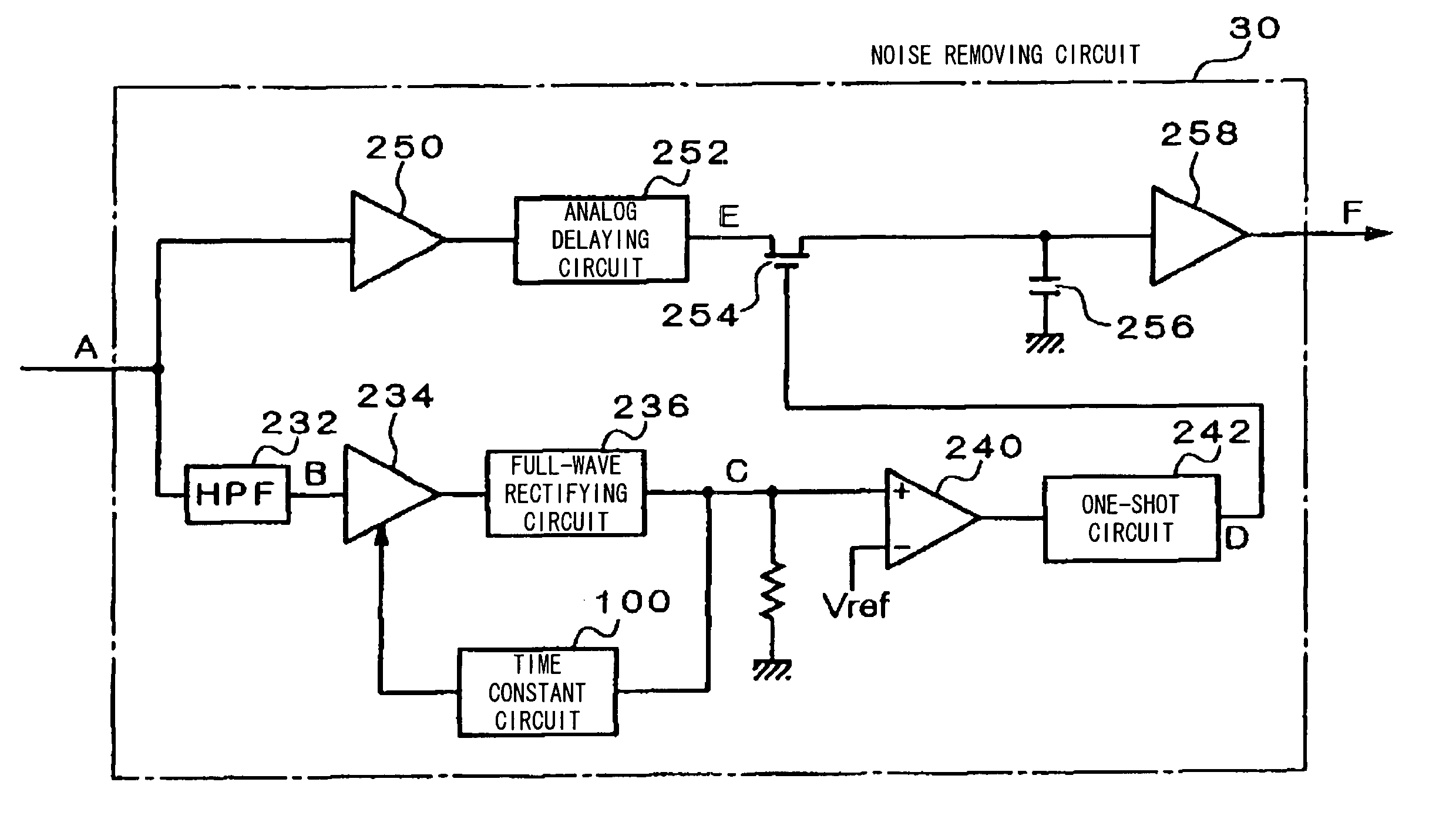
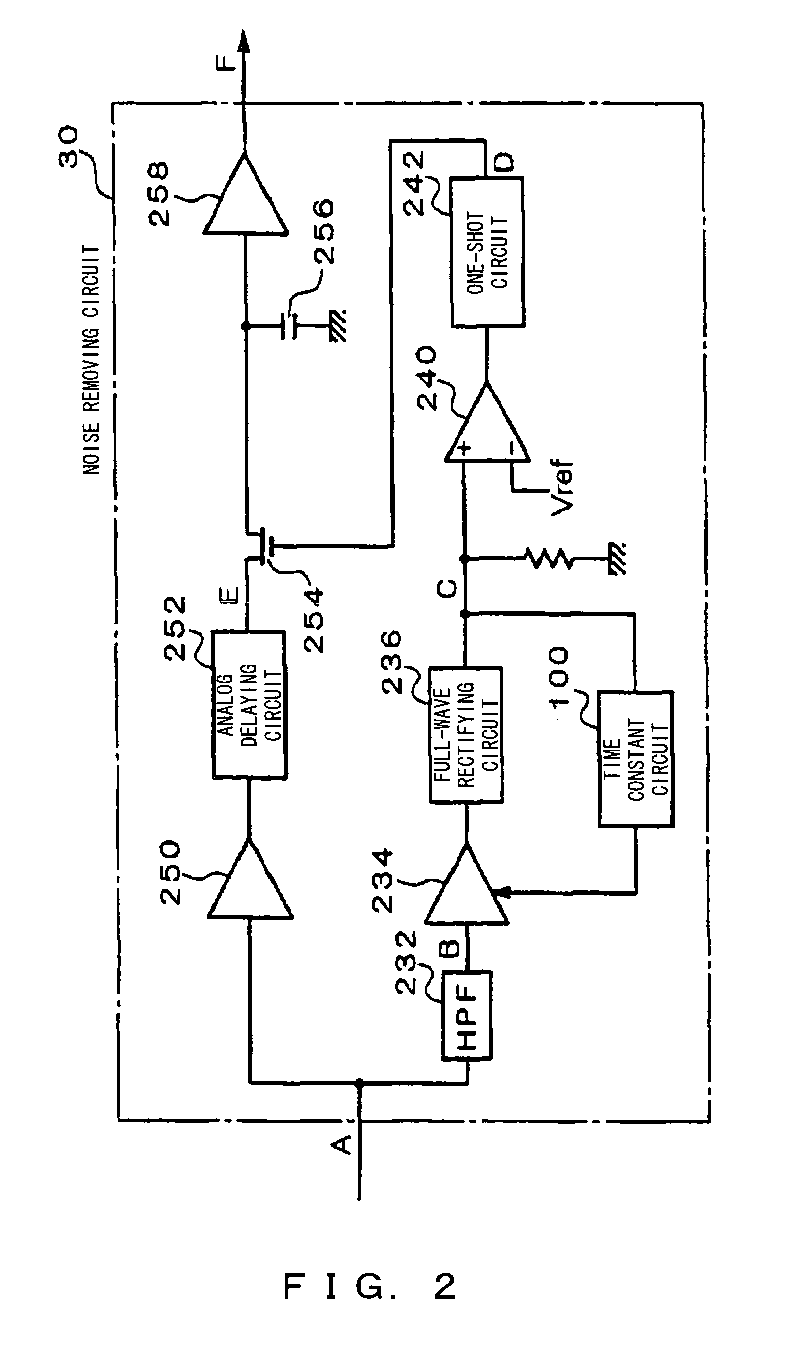
[0023]Hereinafter, a noise removing circuit according to one preferred embodiment, to which the present invention is applied, is described with reference to the drawings.

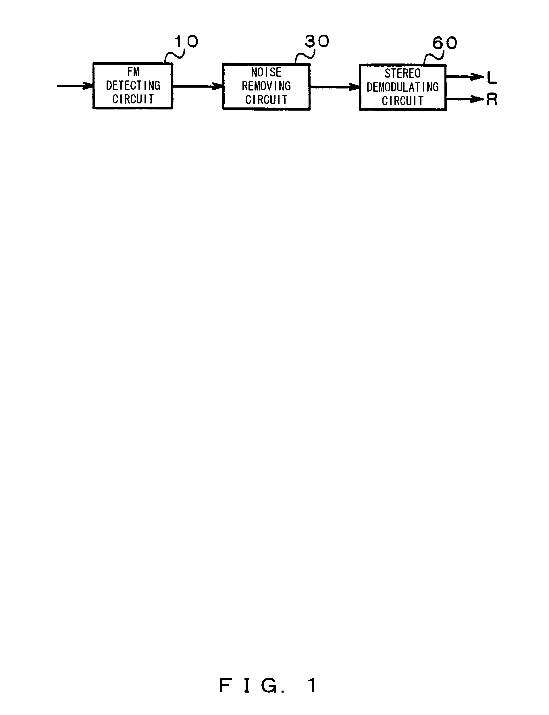
[0024]FIG. 1 shows a partial configuration of an FM receiver including a noise removing circuit according to one preferred embodiment. As shown in FIG. 1, the FM receiver in this preferred embodiment is configured by comprising an FM detecting circuit 10, a noise removing circuit 30, and a stereo demodulating circuit 60. The FM detecting circuit 10 outputs a stereo composite signal by executing an FM detection process for an intermediate frequency signal amplified by an intermediate frequency amplifying circuit (not shown). The noise removing circuit 30 removes noise included in the FM stereo composite signal input from the FM detecting circuit 10. The stereo demodulating circuit 60 executes a stereo demodulation process for separating L and R signals included in the input stereo composite signal.

[0025]FIG. 2 shows ...


PUM


Abstract

An object is to provide a noise removing circuit that can be integrally formed on a semiconductor substrate and can improve the accuracy of noise component removal. The noise removing circuit comprises a highpass filter detecting a noise component included in an input signal, a pulse generating circuit generating a pulse signal corresponding to the detected noise component, an analog delaying circuit 252 delaying the input signal, and an outputting circuit removing the noise component included in the delayed signal according to the output timing of the pulse signal. The analog delaying circuit 252 delays the output timing of the input signal by making switches 51 to 56 electrically continuous in a sequential order, by holding the voltage of the input signal at each time point in a plurality of capacitors 81 to 86, and by extracting the held voltage before being updated by making switches 61 to 66 electrically continuous.

Description

TECHNICAL FIELD[0001]The present invention relates to a noise removing circuit removing a noise component included in a signal in a receiver, etc.BACKGROUND ART[0002]Noise caused by another car-mounted appliance is apt to be mixed into a signal input / output to / from an AM or FM receiver mounted in a car. Accordingly, various types of noise removing circuits are conventionally adopted. As one of examples, there is a method removing noise by extracting a noise component from a signal, by masking part of the signal, which corresponds to the noise component, and by holding the voltage of the immediately preceding input signal. With this method, a pulse signal is generated to mask the noise. However, if attempts are made to mask the noise, timing when the noise occurs and timing when the pulse signal generated based on this noise occurs must be made to match. Since a predetermined amount of time is naturally required to generate the pulse signal, an analog delaying circuit delaying the si...

Claims


Application Information

Patent Timeline
Patent Type & Authority Patents(United States)
IPC IPC(8): H04B1/10H03H11/26H03H19/00H03K5/1252
CPCH03H19/00H03H19/004H03K5/1252H03H11/26H04B1/10
Inventor MIYAGI, HIROSHI
Owner TOYOTA IND CORP
Why Eureka
Try Eureka