
System and method for automatic masking of compressed scan chains with unbalanced lengths

a compression scan chain and automatic masking technology, applied in the field of electronic system testing, can solve the problems of a large amount of data generated, less than 100% of the gates can be tested, and it takes a substantial amount of time to shift the test patterns into the scan chain

Active Publication Date: 2006-11-28
AVAGO TECH INT SALES PTE LTD
View PDF3 Cites 39 Cited by
  • Summary
  • Abstract
  • Description
  • Claims
  • Application Information

AI Technical Summary

Benefits of technology

This approach enables efficient scan testing in unbalanced scan chains by masking bits from shorter segments, reducing the number of shifts required and eliminating ambiguous results, thereby shortening test duration and lowering costs without the need for additional padding bits.

Problems solved by technology

Although an attempt is made to test all of the gates in a modern architecture, for technical reasons, typically less than 100% of the gates can be tested.
However, in spite of this, because of the large number of gates in modern architectures, a tremendous amount of data is generated with each test and a substantial number of test patterns have to be generated to properly test a device.
Since the flip-flops are connected in a serial chain and each bit in the test pattern is shifted into the scan chain at the rate of one bit per clock cycle, when there are tens of millions of bits, it takes a substantial amount of time to shift the test patterns into the scan chain.
The cost of performing the scan chain test is directly proportional to the amount of time required to perform the test.
In addition, the complexity of chips (i.e., ASICs) is increasing.
As the complexity of ASICs increases, the number of flip-flops, and thus the associated scan test length, also increases.
As a result of the fewer, longer scan chains, the cost of the scan test increases.
As a result, although limited input / output pins are available, a large variety of test patterns can be generated to test the targeted faults in a limited amount of time.
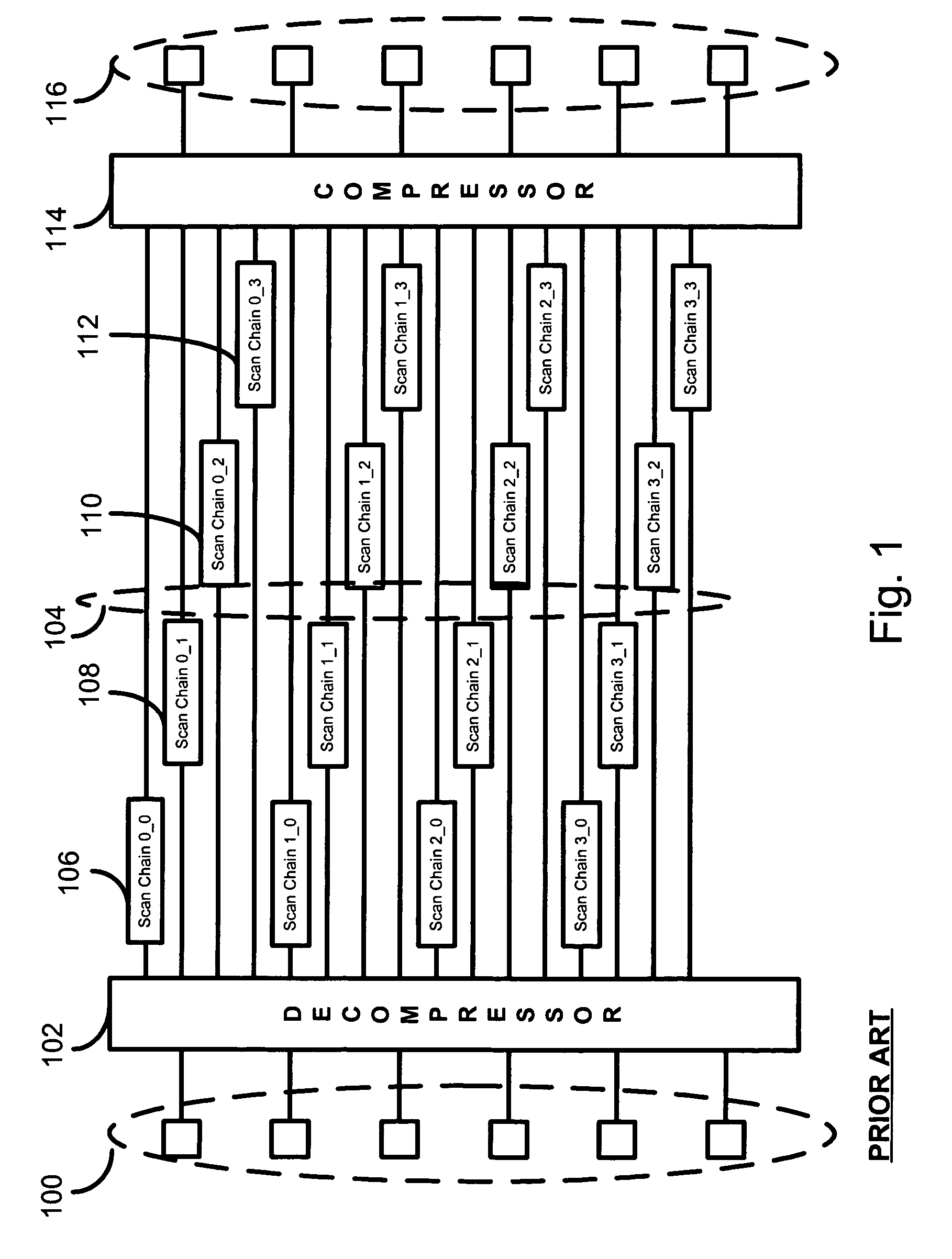
In all of these simple compression schemes, a bit with an unpredictable value (an X) that is shifted out of a segment will render the result of the compressor meaningless, as it becomes impossible to know whether the result is correct or incorrect due to the unpredictable value.
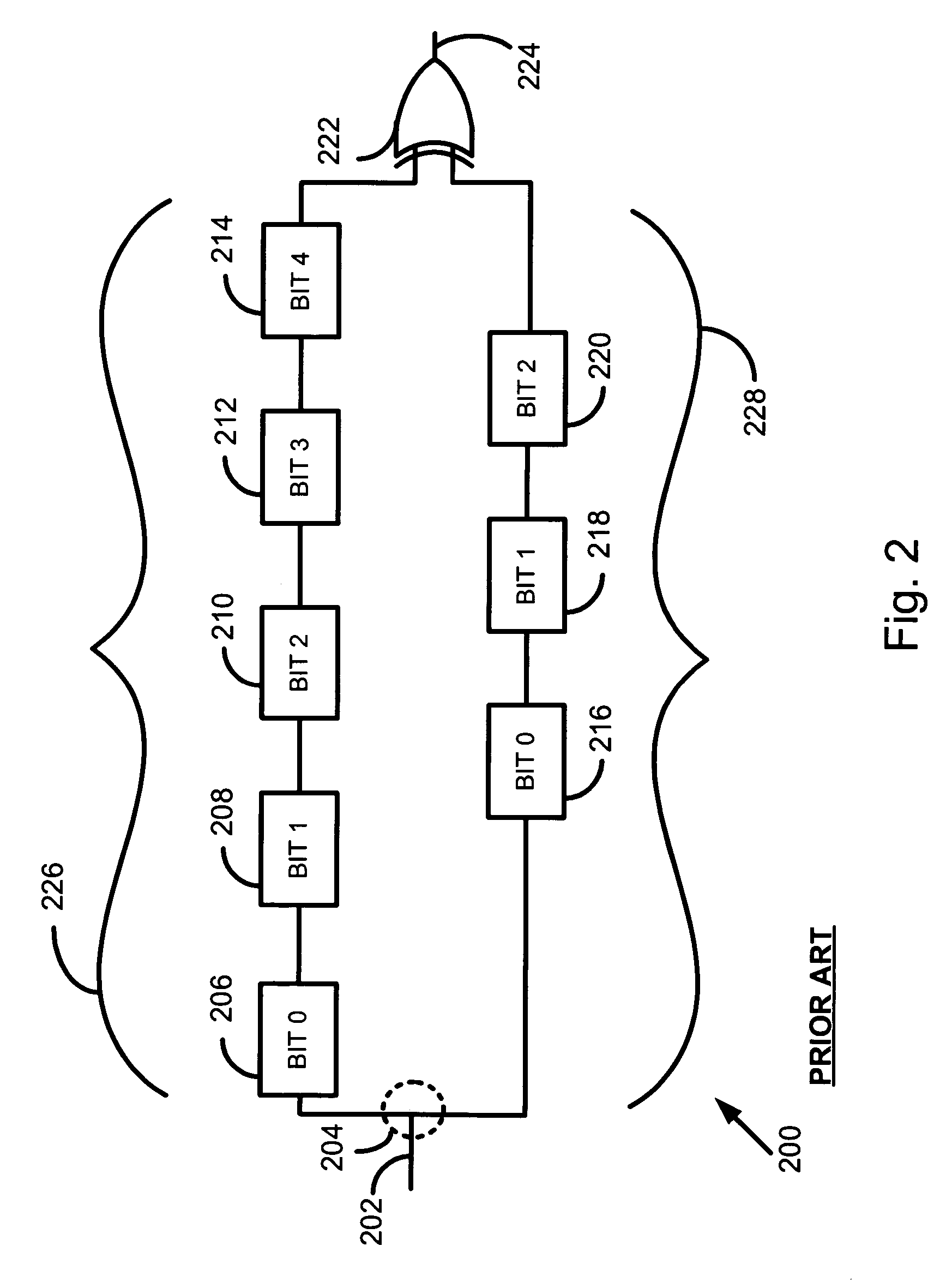
In practice, it is nearly impossible to achieve a balanced scan chain architecture due to imbalances inherent in the physical partitioning of the circuit being scanned.
In the unbalanced case, you have to perform 5 shifts to exercise the longer chain, but shifts 4 and 5 produce potentially ambiguous results from the end of the 3 flip-flop chain.
However, this technique also doubles the tester time needed to perform the test.
However, this approach makes initial chip turn-on or debugging more difficult.
However, this approach increases tester time and cost, though not as much as in the first method.
However, this approach makes the ATPG tool more complicated, and if reordering the tests becomes necessary, the user has to return to the ATPG tool to update the expected results.

Method used


Image

  • System and method for automatic masking of compressed scan chains with unbalanced lengths
  • System and method for automatic masking of compressed scan chains with unbalanced lengths
  • System and method for automatic masking of compressed scan chains with unbalanced lengths

Examples


fourth embodiment

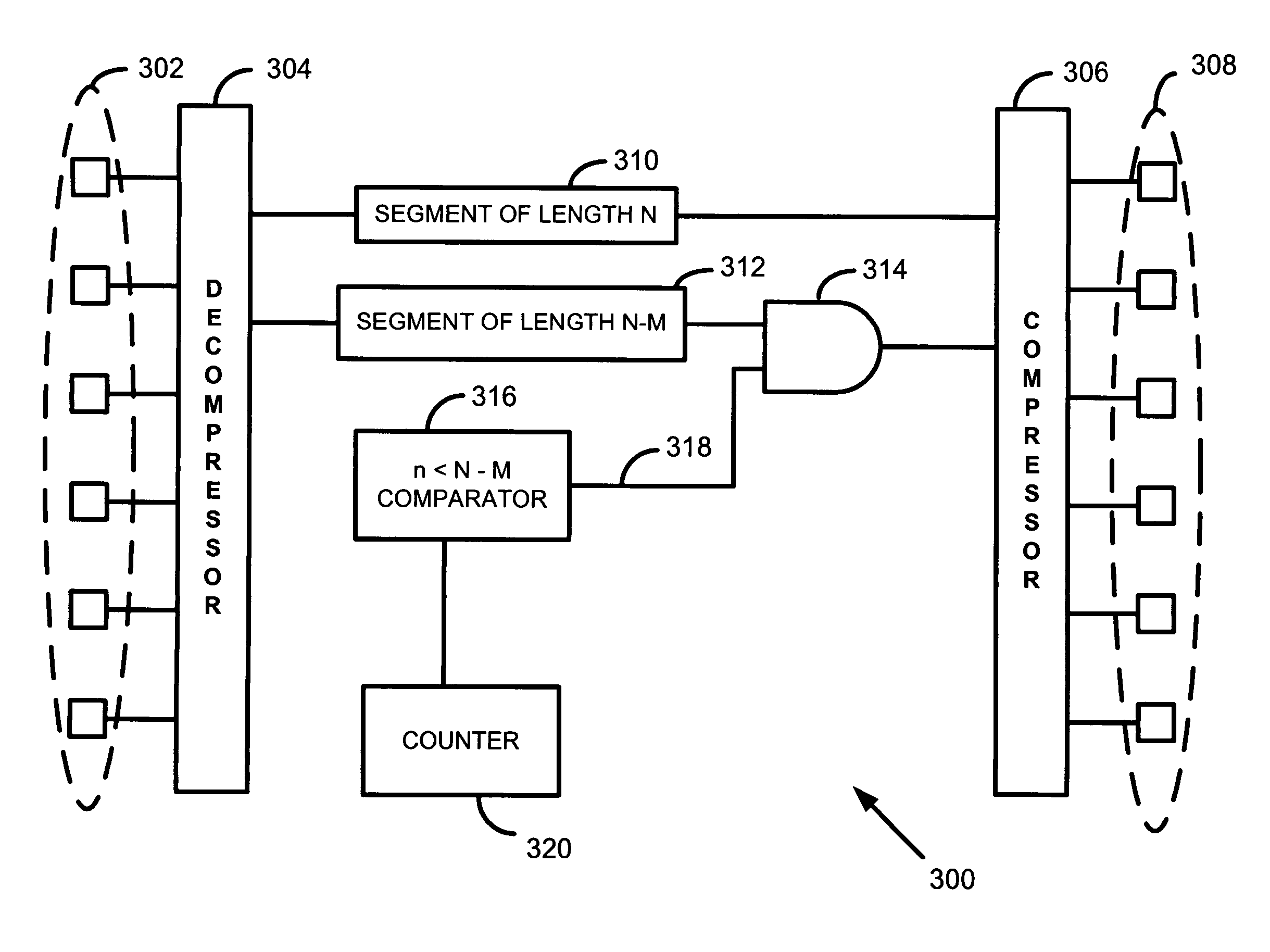
[0061]In a fourth embodiment, comparators that program themselves may be implemented. The comparators may program themselves with the count during a learning phase or training sequence. Implementing comparators that program themselves would require a particular procedure to prepare the chip for testing. In one embodiment, a preparation process may be implemented as follows:[0062]A. Power up the chip. All the flip-flops are assumed to hold random values.[0063]B. Shift a sufficient number of zeros to be certain that all the flip-flops contain zero.[0064]C. Assert a “learning mode” signal, either directly from the outside world or through a TAP.[0065]D. Shift in a pattern of all ones. When each comparator sees a value of one appear at the end of the segment it is associated with, it stores the current value of the counter as the value to compare against, thus completing the training.

[0066]FIG. 4 displays a flow diagram of a method of operating a scan chain architecture including a sing...

second embodiment

[0078]In a second embodiment, M1=M2. In this variation, a single comparator is required, but two masking gates, one for each short chain, are required. The sequence is the same as for a single short segment, except after N−M shifts, the outputs of both short chains are masked off and the compressor 506 sees only zeros for those chains. This allows the sharing of the comparator logic. Otherwise, it is simply a degenerate case of the two short-chains example.

[0079]It should be appreciated that both variations of the two short scanchain segments can be combined to handle any number of short scan chains. For each short length (N−Mi), a comparator is required. For each chain of that length, a masking gate connected to the mask signal from that comparator is required.

[0080]A number of variations may be implemented using the scan chain architecture 500 or a variation of the scan chain architecture 500. A number of adaptive and / or learning comparators may be implemented in scan chain archit...


PUM


Abstract

A scan test architecture is implemented. The scan test architecture provides a method of performing scan test of unbalanced scan chains. The scan test architecture generates a control signal (i.e., masking signal) to mask bits in an unbalanced scan chain. In one embodiment, the control signal is generated with a logic gate, a comparator, and a counter.

Description

FIELD OF THE INVENTION[0001]This invention relates to electronics systems. Specifically, the present invention relates to electronic system testing.DESCRIPTION OF THE RELATED ART[0002]Scan tests are implemented to test faulty circuit behavior, such as behavior caused by manufacturing defects in digital logic based devices. For example, modern microprocessors are implemented using tens of millions of logic gates. Scan tests are used to test the logic gates for faults.[0003]In a conventional scan test, a test pattern is generated to test a prospective device. The test pattern may include a sequence of zeros and ones defined to test various logic gates. An automated test pattern generator (ATPG) is typically used to generate the test pattern. The ATPG analyzes a circuit model (i.e., called a netlist) of a digital logic based device such as a microprocessor (i.e., chip) and identifies a set of potential fault locations or sites on the chip. The ATPG then generates the test patterns nece...

Claims


Application Information

Patent Timeline
Patent Type & Authority Patents(United States)
IPC IPC(8): G01R31/28
CPCG01R31/318547
Inventor BRATT, JOHN T.REARICK, JEFFREY R.
Owner AVAGO TECH INT SALES PTE LTD
Learn More