In situ particle monitoring for defect reduction

a particle monitoring and defect reduction technology, applied in semiconductor/solid-state device testing/measurement, optical investigation of flaws/contamination, instruments, etc., can solve problems such as contaminating the thin photoresist film on the wafer, defects in the wafer, and virtually useless wafers, so as to remove excessive contaminates

Inactive Publication Date: 2006-12-05
ADVANCED MICRO DEVICES INC
View PDF17 Cites 14 Cited by
  • Summary
  • Abstract
  • Description
  • Claims
  • Application Information

AI Technical Summary

Benefits of technology

[0008]The monitoring system can also be utilized in providing a warning system to a user if the particle count exceeds a predetermined level. The warning system could also include an exhaust fan that turns on during an alarm condition to remove excessive contaminates found in the aerosols. The present invention also implements the monitoring system into a control system for controlling the contaminated particles suspended in the aerosols. A control signal can be formulated corresponding to the contaminated particle count and communicated to an exhaust flow control valve that controls an exhaust fan that is in communication with the chamber of cup. In this way, the contaminated particle count can be automatically controlled before, during and after the photoresist coating and / or development process.

Problems solved by technology

Contaminant particles residing or introduced into the chamber where the photoresist is applied are a major cause of defects in wafers.
In some cases, the contaminant particles can have thicknesses as large as the thicknesses of the wafers making the wafers virtually useless.
Aerosol not removed by a cleaning system (e.g., vacuum system) may contribute to contaminating the thin photoresist film on the wafer.

Method used


Image

  • In situ particle monitoring for defect reduction
  • In situ particle monitoring for defect reduction
  • In situ particle monitoring for defect reduction

Examples


Embodiment Construction

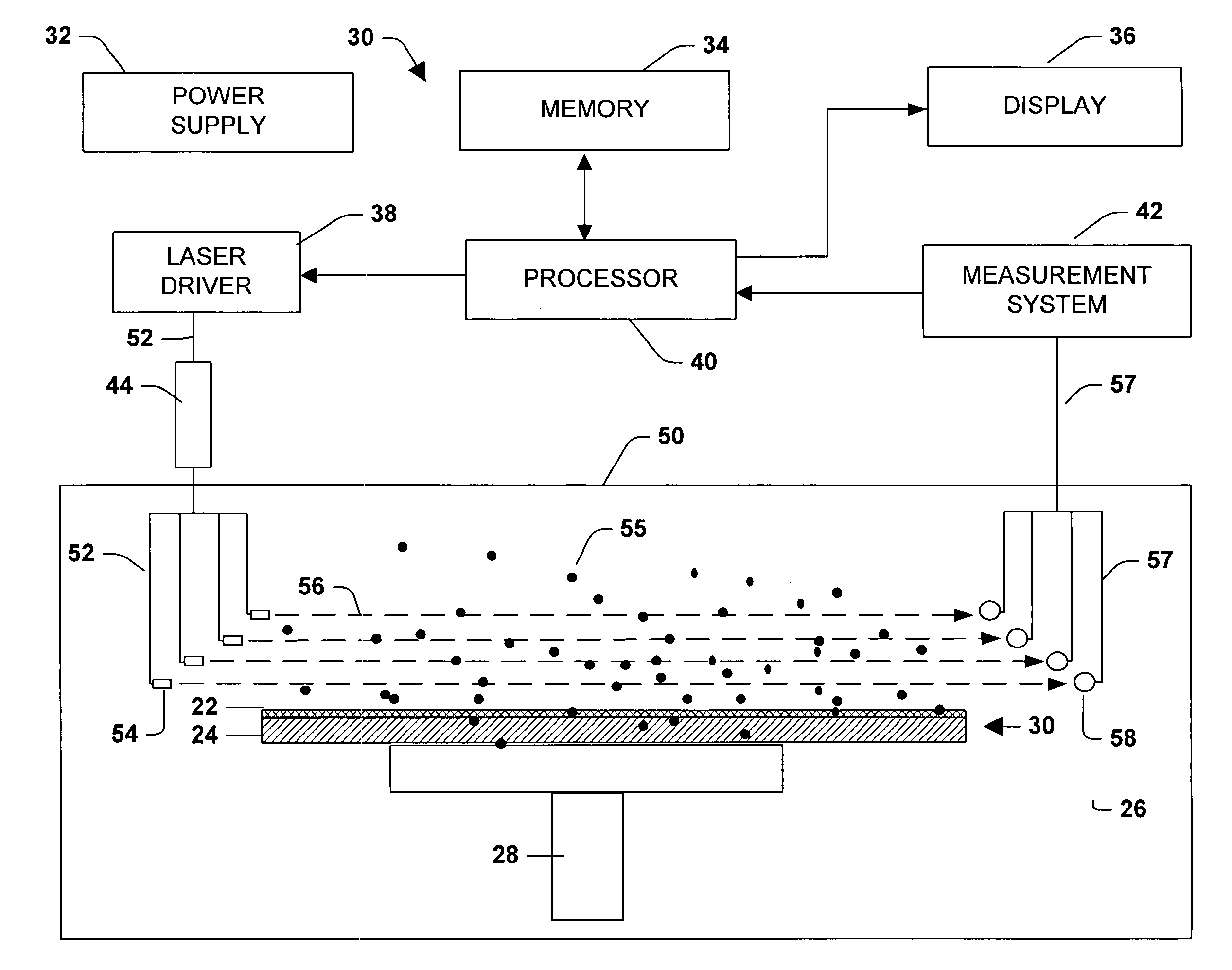
[0022]The present invention will now be described with reference to the drawings, wherein like reference numerals are used to refer to like refer to like elements throughout. The present invention will be described with reference to a system and method for monitoring and controlling the contaminant particle count contained in an aerosol during a photoresist coating and / or development process of a semiconductor. The following detailed description is of the best modes presently contemplated by the inventors for practicing the invention. It should be understood that the description of these preferred embodiments are merely illustrative and that they should not be taken in a limiting sense.

[0023]Referring initially to FIG. 1, a system 30 for applying uniformly a photoresist material layer 22 on a substrate 24 to form a wafer 20 is shown. The substrate 24 is vacuum held onto a rotating chuck 26, which is spin rotated by a shaft 28 driven by a motor (not shown). The wafer 20, the rotating...


PUM

PropertyMeasurementUnit
heightsaaaaaaaaaa
light transmissionsaaaaaaaaaa
light intensityaaaaaaaaaa

Abstract

A system and method is provided for monitoring and controlling the contaminant particle count contained in an aerosol during a photoresist coating and/or development process of a semiconductor. The monitoring system monitors the contaminate particle count present in the environment of the photoresist coating and/or development process, such as in a process chamber or a cup, enclosing the wafer during the process. The present invention employs in situ laser scattering or laser doppler anemometry techniques to detect the particle count level in the chamber or cup. A plurality of lasers and detectors can be positioned at different heights in or outside of a chamber or cup to facilitate detecting particles at different height levels. A laser could be used in conjunction with mirrors to provide a similar measurement. The particle count level can be used to compare with the defect level, so that it can be determined if a cleaner environment and/or process should be implemented.

Description

TECHNICAL FIELD[0001]The present invention generally relates to semiconductor processing, and in particular to a system and method for measuring and controlling contaminates in a deposition chamber utilized in a photolithographic process.BACKGROUND OF THE INVENTION[0002]In the semiconductor industry, there is a continuing trend toward higher device densities. To achieve these high densities there has been and continues to be efforts toward scaling down device dimensions (e.g., at submicron levels) on semiconductor wafers. In order to accomplished such high device packing density, smaller and smaller features sizes are required. This may include the width and spacing of interconnecting lines, spacing and diameter of contact holes, and the surface geometry such as corners and edges of various features.[0003]The requirement of small features with close spacing between adjacent features requires high resolution photolithographic processes. In general, lithography refers to processes for...

Claims


Application Information

Patent Timeline
Patent Type & Authority Patents(United States)
IPC IPC(8): G01N21/00
CPCG01N15/0205G01N21/5907G01N21/94G01N21/9501H01L22/10G01N2021/5961G01N2021/8411
Inventor TEMPLETON, MICHAEL K.RANGARAJAN, BHARATH
Owner ADVANCED MICRO DEVICES INC
Why Eureka
Try Eureka