Global shape definition method for scatterometry

Active Publication Date: 2006-12-05
THERMA WAVE INC
View PDF22 Cites 23 Cited by
  • Summary
  • Abstract
  • Description
  • Claims
  • Application Information

AI Technical Summary

Benefits of technology

[0015]The present invention also provides an interactive environment for building and evaluating scatterometry models based on the global shape definition method. The interactive environment allows a user to specify multilayer scatterometry models. The user can add shape profiles by adding groups of control points. Once a model has been defined, the interactiv

Problems solved by technology

Complex samples, such as the sample shown in FIG. 3 require correspondingly complex modeling techniques.
The slab-based technique necessarily introduces a degree of roughness into the resulting model.
At the same

Method used


Image

  • Global shape definition method for scatterometry
  • Global shape definition method for scatterometry
  • Global shape definition method for scatterometry

Examples


Embodiment Construction

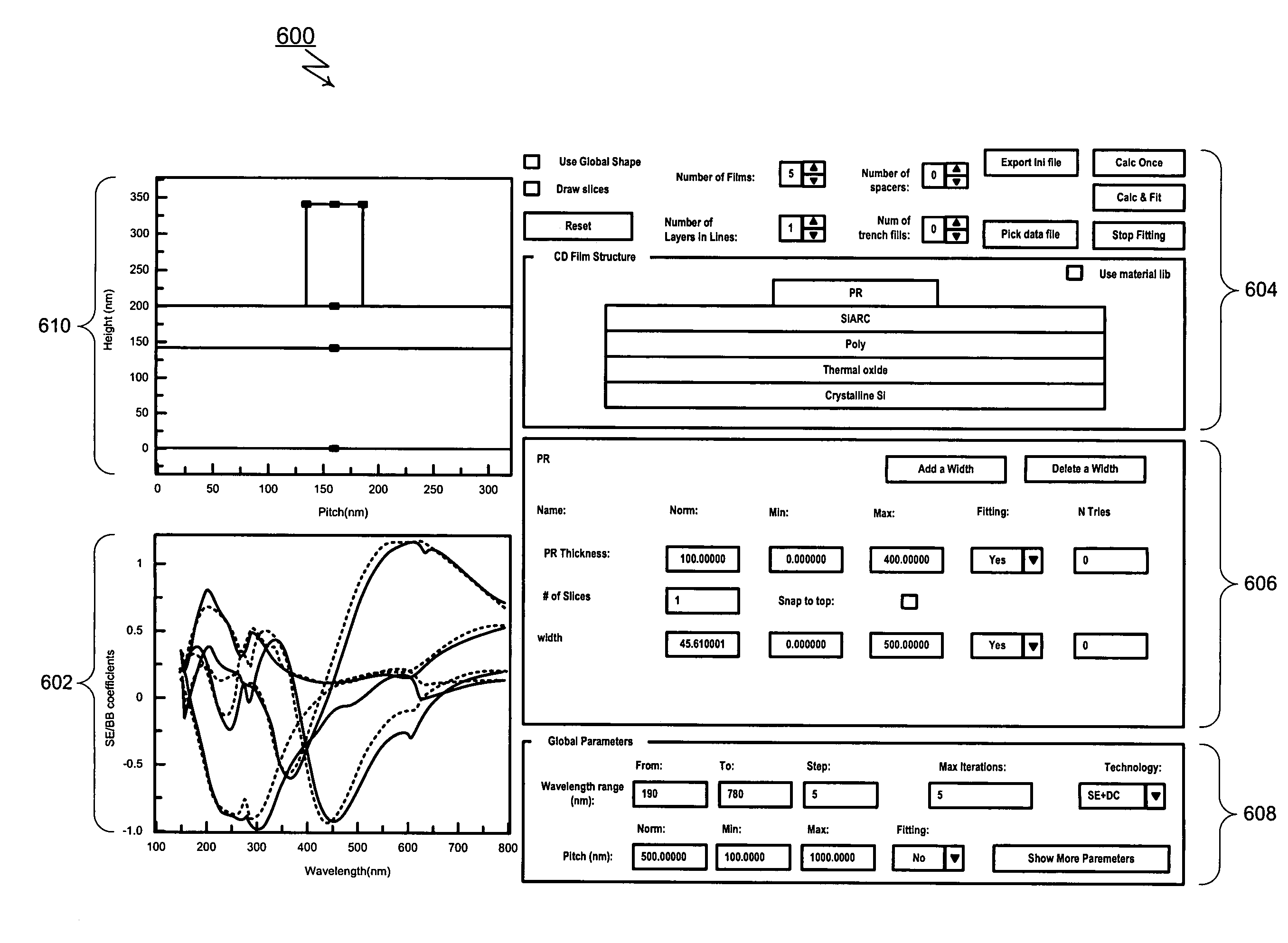
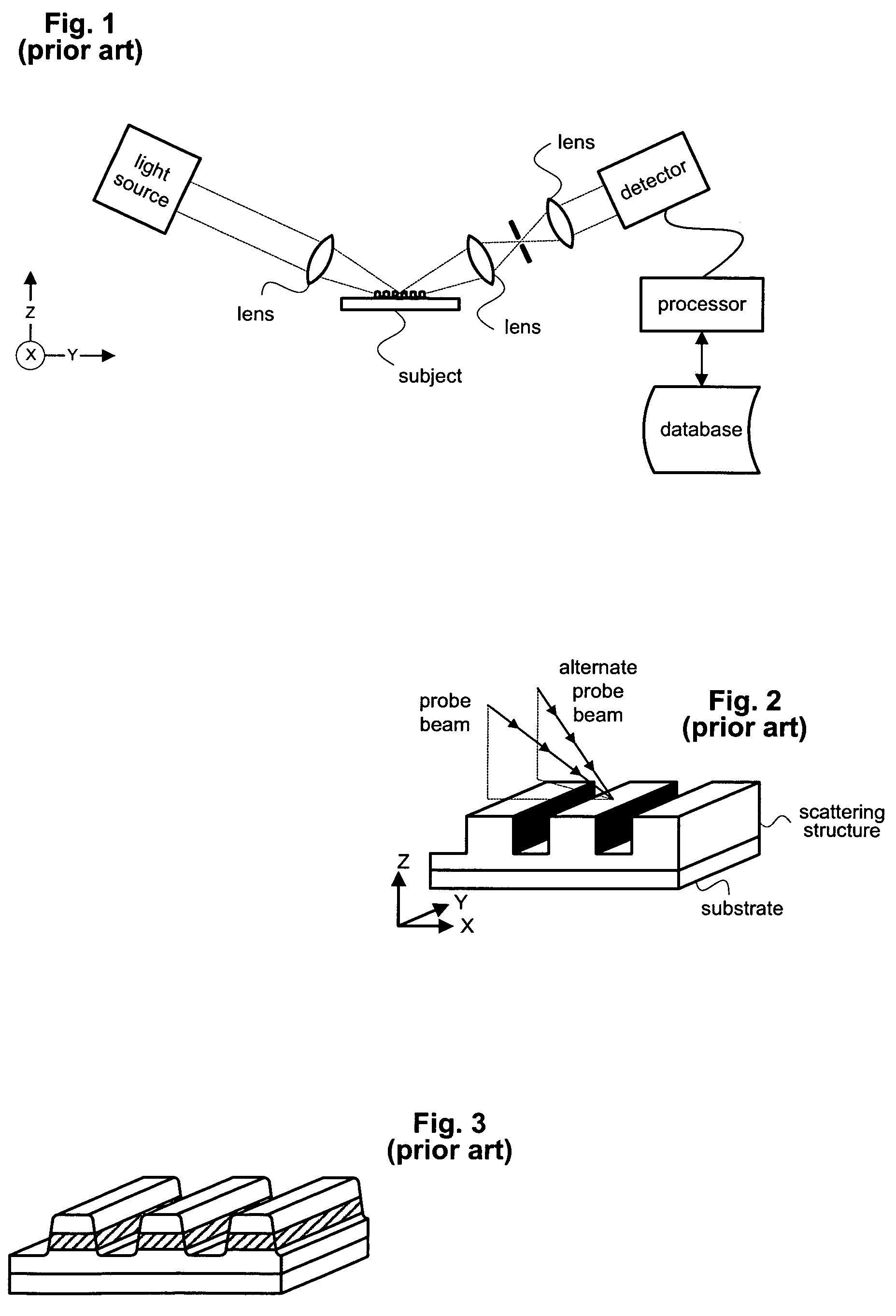
[0034]The present invention provides a global shape definition method for modeling samples. For typical applications, the sample to be modeled is a semiconductor wafer of the type generally shown in FIGS. 2 and 3 and includes a scattering structure formed on one or more underlying layers. The lowermost of the underlying layers is commonly referred to as a substrate. The scatting structure is covered by an incident medium that is typically air but may be vacuum, gas, liquid, or solid (such as an overlaying layer or layers). In the most typical case, the scattering structure is a grating consisting of a periodic series of lines. By appropriate generalizations, other isolated or periodic features may also be modeled.

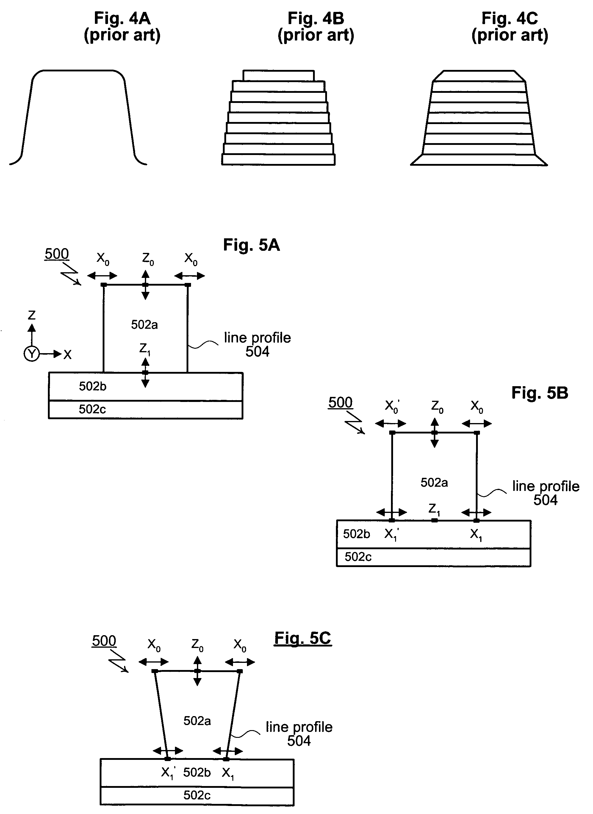
[0035]For the global shape definition method, a control-point based approach is used to define the profiles (i.e., the cross-sectional outlines) of geometric shapes within the sample. FIG. 5A shows a sample 500 modeled using this approach. For this particular example, sampl...


PUM


Abstract

A method for modeling samples includes the use of control points to define lines profiles and other geometric shapes. Each control point used within a model influences a shape within the model. Typically, the control points are used in a connect-the-dots fashion where a set of dots defines the outline or profile of a shape. The layers within the sample are typically modeled independently of the shape defined using the control points. The overall result is to minimize the number of parameters used to model shapes while maintaining the accuracy of the resulting scatterometry models.

Description

PRIORITY CLAIM[0001]The present application claims priority to U.S. Provisional Patent Application Ser. No. 60 / 463,791, filed Apr. 18, 2003, the disclosure of which is incorporated in this document by reference.TECHNICAL FIELD[0002]The subject invention relates generally to optical methods for inspecting and analyzing semiconductor wafers and other samples. In particular, the subject invention relates to methods for modeling samples for scatterometry and other applications.BACKGROUND OF THE INVENTION[0003]As semiconductor geometries continue to shrink, manufacturers have increasingly turned to optical techniques to perform non-destructive inspection and analysis of semiconductor wafers. Optical techniques typically apply an incident field (often referred to as a probe beam) to a sample and then detect and analyze the reflected energy. This type of inspection and analysis is known as optical metrology and is performed using a range of optical techniques. Scatterometry is a specific t...

Claims


Application Information

Patent Timeline
IPC IPC(8): G01B11/00G06F17/00G01N21/47
CPCG01N21/4788
Inventor OPSAL, JONCHU, HANYOUCAO, XUELONGWEN, YOUXIAN
Owner THERMA WAVE INC
Why Eureka
Try Eureka