Method and apparatus for configuring a programmable logic device

a logic device and programmable logic technology, applied in the field of programmable logic devices, can solve the problems of affecting the cost of a separate memory device for each fpga, and the limitation of fpgas that can affect the design's decision to us

Inactive Publication Date: 2006-12-05
MCDATA SERVICES CORP +1
View PDF18 Cites 32 Cited by
  • Summary
  • Abstract
  • Description
  • Claims
  • Application Information

AI Technical Summary

Benefits of technology

[0008]The present invention provides a method and apparatus that enables a user to program multiple programmable logic devices with a minimum number of memory devices.
[0010]The above can be achieved through the use of a novel combination of a single memory device and a processor to program or configure multiple programmable logic devices. The memory serves as the location where the configuration code for the FPGAs is stored. This arrangement enables the user to save and potentially open up valuable real estate and reduces the drain on the power supply on a circuit board within a system. In accordance with one embodiment of the present invention, an apparatus for configuring a first programmable device includes a microprocessor, a second programmable logic with an interface logic to link the microprocessor and the first programmable logic device and a status check that is linked to the second programmable logic device. The status check determines the condition of the first programmable logic device. The final element is a memory device that is linked to the microprocessor. The memory device provides a configuration code for the first programmable logic device. In this embodiment, the first programmable logic device is a field programmable gate array (FPGA). while the second programmable device is a complex programmable logic device (CPLD). The FPGN's configuration code that is stored in the microprocessor's memory device can changed via the microprocessor's communication's port. This allows new configurations to be downloaded to the memory device.

Problems solved by technology

However, there are limitations in FPGAs that can affect a designer's decision to use them.
One of the disadvantages of using FPGAs is that currently each FPGA requires its own memory device.
One disadvantage to having a separate memory device for each FPGA is the overall cost.
Furthermore, memory prices have a tendency to fluctuate.
The other disadvantage with the individual memory devices is the amount of space required on the circuit board.
The addition of multiple FPGAs does not help the problem if each FPGA is required to have its own memory device.
Furthermore, there is a redundancy in the system with memory devices storing the identical configuration logic for each FPGA.
Finally, an integrated chip such as an FPGA can malfunction and disrupt the operation of a system or device.
With FPGAs, it is not possible to check the status or condition of the FPGA without pulling the FPGA from its slot.
Further complicating the problem is the ability to detect whether the FPGA is the cause of the malfunction.

Method used


Image

  • Method and apparatus for configuring a programmable logic device
  • Method and apparatus for configuring a programmable logic device
  • Method and apparatus for configuring a programmable logic device

Examples


Embodiment Construction

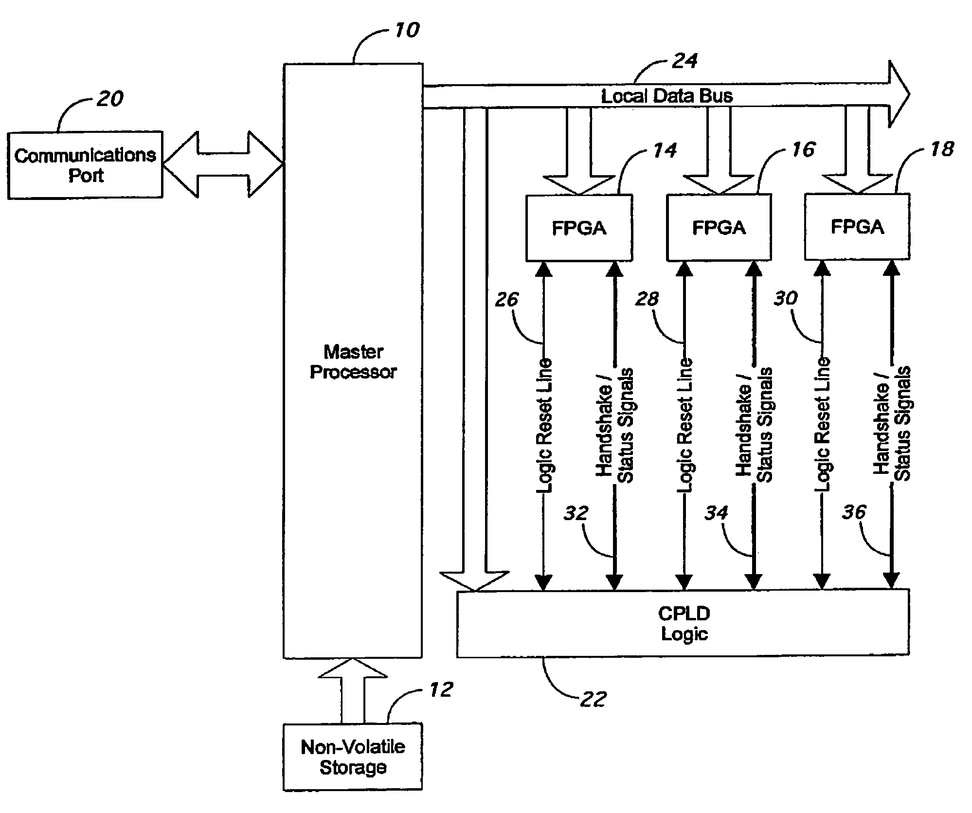
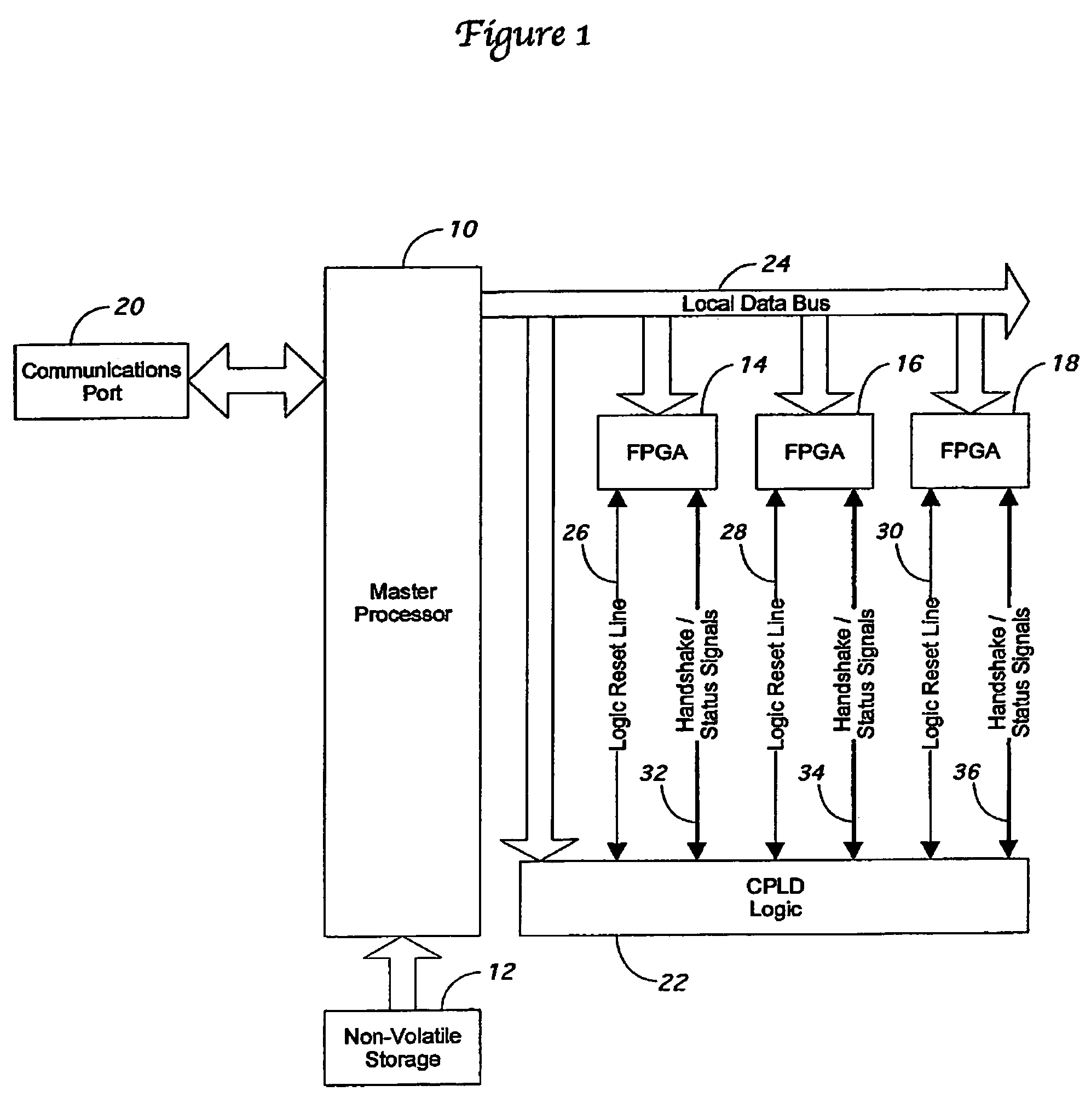
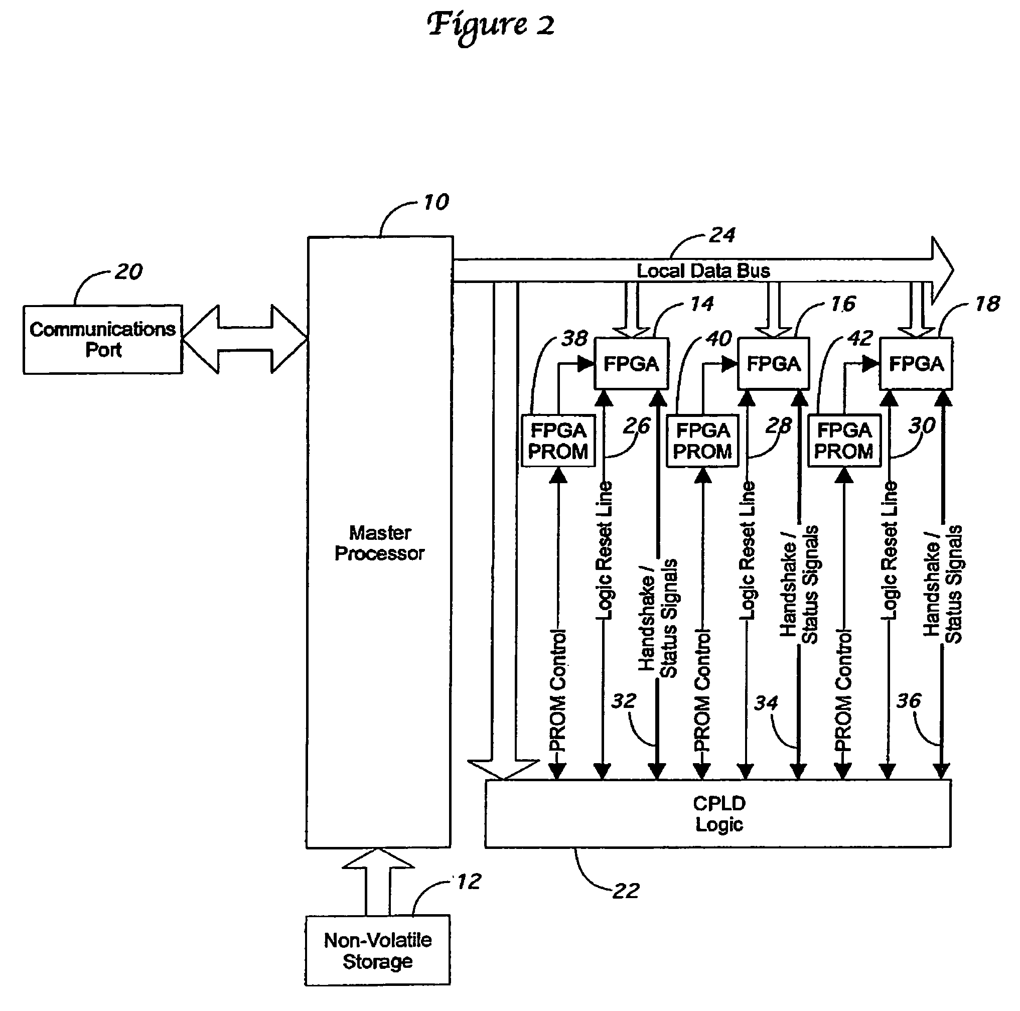
[0027]A preferred embodiment of the present invention provides a method and apparatus that enables a user to check the status of a programmable logic device and program or configure this device in a manner that is intended or that the user desires. A preferred embodiment of the present inventive apparatus and method is illustrated in FIG. 1. In FIG. 1, the present invention includes a microprocessor 10, which is linked to storage device 12. The storage device 12 contains the application computer executable code, such as the boot code, and the configuration computer code for the field programmable gate arrays (FPGA) 14,16,18.

[0028]In the preferred embodiment, the storage device is non-volatil memory.

[0029]The preferred embodiment is connected to a communications port 20. In the preferred embodiment, the microprocessor 10 is linked to the communications port 20. The communications port 20 enables differing FPGA configurations to be downloaded to the storage device 12 via the microproc...


PUM


Abstract

A method and apparatus for configuring multiple first programmable logic devices from a single memory includes a microprocessor, and a second programmable logic device containing the interface logic for the first programmable device and the microprocessor. The present invention allows multiple FPGAs to be programmed from a single memory structure under the control of the microprocessor thereby using fewer components than systems dedicating a separate memory to each FPGA. A communications port allows new configurations to be downloaded to the microprocessor memory. In addition, the present invention can be used in combination with standard systems with each FPGA having its own memory, with the microprocessor being able to select between the central microprocessor memory and the local memory for programming each FPGA.

Description

PRIORITY[0001]This application claims priority to the provisional U.S. patent application entitled, A Method and Apparatus for Configuring Programmable Logic Devices, filed Nov. 7, 2002, having a Ser. No. 60 / 424,333, the disclosure of which is hereby incorporated by reference.FIELD OF THE INVENTION[0002]The present invention relates generally to programmable logic devices. More particularly, the present invention relates to using, configuring and identifying logic devices with a minimum number of memory devices.BACKGROUND OF THE INVENTION[0003]The Field Programmable Gate Array (FPGA) is an integrated circuit (IC) that can be programmed in the field after manufacture. FPGAs are similar in principle to, but have vastly wider potential application than, programmable read-only memory (PROM) chips. FPGAs are used by engineers in the design of specialized ICs that can later be produced hard-wired in large quantities for distribution to computer manufacturers and end users. Ultimately, FPG...

Claims


Application Information

Patent Timeline
Patent Type & Authority Patents(United States)
IPC IPC(8): G06F17/50G01R31/28G06F1/24G06F7/38H03K19/173G06F15/78H04L29/08
CPCG06F15/7867G06F17/5054H04L67/34H04L69/329G06F30/34
Inventor HORANZY, JOSEPH
Owner MCDATA SERVICES CORP
Why Eureka
Try Eureka